
Page 44 - Semiconductor Manufacturing Handbook
P. 44
Geng(SMH)_CH04.qxd 04/04/2005 19:36 Page 4.7
COPPER, LOW-k DIELECTRICS, AND THEIR RELIABILITY
COPPER, LOW-κ DIELECTRICS, AND THEIR RELIABILITY 4.7
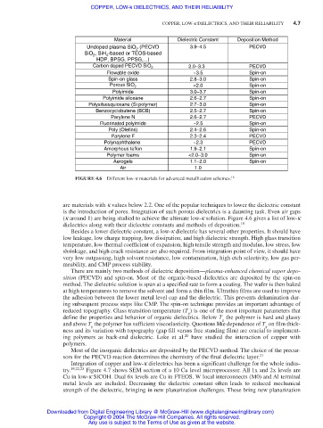
Material Dielectric Constant Deposition Method
Undoped plasma SiO (PECVD 3.9−4.5 PECVD
2
SiO , SiH -based or TEOS-based
2
4
HDP, BPSG, PPSG,...)
Carbon doped PECVD SiO 2 2.0−3.3 PECVD
Flowable oxide ~3.5 Spin-on
Spin-on glass 2.8−3.0 Spin-on
Porous SiO <2.0 Spin-on
2
Polyimide 3.0−3.7 Spin-on
Polyimide siloxane 2.6−2.7 Spin-on
Polysilsesquioxane (Si polymer) 2.7−3.0 Spin-on
Benzocyclobutene (BCB) 2.5−2.7 Spin-on
Parylene N 2.6−2.7 PECVD
Fluorinated polyimide ~2.5 Spin-on
Poly (Olefins) 2.4−2.6 Spin-on
Parylene F 2.3−2.4 PECVD
Polynaphthalene ~2.3 PECVD
Amorphous teflon 1.9−2.1 Spin-on
Polymer foams <2.0−3.0 Spin-on
Aerogels 1.1−2.0 Spin-on
Air 1.0
FIGURE 4.6 Different low-κ materials for advanced metallization schemes. 18
are materials with κ values below 2.2. One of the popular techniques to lower the dielectric constant
is the introduction of pores. Integration of such porous dielectrics is a daunting task. Even air gaps
(k around 1) are being studied to achieve the ultimate low-k solution. Figure 4.6 gives a list of low-k
dielectrics along with their dielectric constants and methods of deposition. 18
Besides a lower dielectric constant, a low-k dielectric has several other properties. It should have
low leakage, low charge trapping, low dissipation, and high dielectric strength. High glass transition
temperature, low thermal coefficient of expansion, high tensile strength and modulus, low stress, low
shrinkage, and high crack resistance are also required. From integration point of view, it should have
very low outgassing, high solvent resistance, low contamination, high etch selectivity, low gas per-
meability, and CMP process stability.
There are mainly two methods of dielectric deposition—plasma-enhanced chemical vapor depo-
sition (PECVD) and spin-on. Most of the organic-based dielectrics are deposited by the spin-on
method. The dielectric solution is spun at a specified rate to form a coating. The wafer is then baked
at high temperatures to remove the solvent and form a thin film. Ultrathin films are used to improve
the adhesion between the lower metal level cap and the dielectric. This prevents delamination dur-
ing subsequent process steps like CMP. The spin-on technique provides an important advantage of
reduced topography. Glass transition temperature (T ) is one of the most important parameters that
g
define the properties and behavior of organic dielectrics. Below T the polymer is hard and glassy
g
and above T the polymer has sufficient viscoelasticity. Questions like dependence of T on film thick-
g g
ness and its variation with topography (gap fill versus free standing film) are crucial to implement-
ing polymers as back-end dielectric. Loke et al. 20 have studied the interaction of copper with
polymers.
Most of the inorganic dielectrics are deposited by the PECVD method. The choice of the precur-
sors for the PECVD reaction determines the chemistry of the final dielectric layer. 21
Integration of copper and low-k dielectrics has been a significant challenge for the whole indus-
try. 19,22,23 Figure 4.7 shows SEM section of a 10 Cu level microprocessor. All 1x and 2x levels are
Cu in low-k SiCOH. Dual 6x levels are Cu in FTEOS. W local interconnects (M0) and Al terminal
metal levels are included. Decreasing the dielectric constant often leads to reduced mechanical
strength of the dielectric, bringing in new planarization challenges. These bring new planarization
Downloaded from Digital Engineering Library @ McGraw-Hill (www.digitalengineeringlibrary.com)
Copyright © 2004 The McGraw-Hill Companies. All rights reserved.
Any use is subject to the Terms of Use as given at the website.