
Page 45 - Semiconductor Manufacturing Handbook
P. 45
Geng(SMH)_CH04.qxd 04/04/2005 19:36 Page 4.8
COPPER, LOW-k DIELECTRICS, AND THEIR RELIABILITY
4.8 SEMICONDUCTOR FUNDAMENTALS AND BASIC MATERIALS
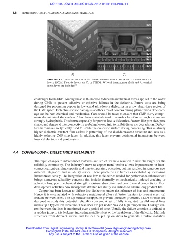
(a) (b)
FIGURE 4.7 SEM sections of a 10-Cu-level microprocessor. All 1x and 2x levels are Cu in
low-κ SiCOH. Dual 6x levels are Cu in FTEOS. W local interconnects (M0) and Al terminal
metal levels are included. 19
challenges to the table. Among these is the need to reduce the mechanical forces applied to the wafer
during CMP, to prevent adhesive or cohesive failures in the dielectric. Future tools are being
designed for processing copper in low-k and ultra-low-k dielectrics in a low shear-force region of
the CMP space. Dielectric surface damage is another area of concern during planarization. The dam-
age can be both chemical and mechanical. Care should be taken to ensure that CMP slurry compo-
nents do not attack the surface. Also, these materials tend to absorb a lot of moisture, but some are
strongly hydrophobic. This is true especially for porous low-k dielectrics. Factors like pore size, pore
shape, and degree of interconnectivity are being looked into to inhibit dielectric degradation. Defect-
free hardmasks are typically used to isolate the dielectric surface during processing. This relatively
higher dielectric constant film assists in patterning of the dual-damascene structure and acts as a
highly selective CMP stop layer. In addition, this layer prevents detrimental interactions between
low-k dielectrics and photoresists.
4.4 COPPER/LOW-k DIELECTRICS RELIABILITY
The rapid changes in interconnect materials and structures have resulted in new challenges for the
reliability community. The industry’s move to copper metallization allows improvements in inter-
connect current-carrying capacity and high-temperature operation, but has resulted in numerous new
material integration and reliability issues. These problems are further exacerbated by increasing
interconnect density. The integration of new low-k dielectrics needed for performance enhancement
brings numerous reliability concerns that include thermally or mechanically induced cracking or
adhesion loss, poor mechanical strength, moisture absorption, and poor thermal conductivity. Most
development activities now incorporate detailed reliability evaluations to ensure long product life.
Copper has been known to diffuse into dielectrics under the influence of bias and temperature.
Hence it is encapsulated with refractory metal/metal alloys diffusion barriers to prevent electrical
leakage between lines. The top surface is capped to prevent interlayer problems. TDDB stresses are
designed to study this potential reliability concern. A set of fully integrated parallel metal lines
makes up a typical test structure. These lines are put under bias and high temperature. Leakage cur-
rent between the lines is monitored over a period of time. Usually the failure criterion is defined as
a sudden jump in this leakage, indicating metallic short or the breakdown of the dielectric. Multiple
structures from different wafers and lots can be put up on stress to generate a failure statistics.
Downloaded from Digital Engineering Library @ McGraw-Hill (www.digitalengineeringlibrary.com)
Copyright © 2004 The McGraw-Hill Companies. All rights reserved.
Any use is subject to the Terms of Use as given at the website.