
Page 48 - Semiconductor Manufacturing Handbook
P. 48
Geng(SMH)_CH04.qxd 04/04/2005 19:36 Page 4.11
COPPER, LOW-k DIELECTRICS, AND THEIR RELIABILITY
COPPER, LOW-κ DIELECTRICS, AND THEIR RELIABILITY 4.11
Stress voiding is another reliability concern for copper/low-κ interconnect systems. Due to the mis-
match in the thermal expansion coefficient, the interconnect’s final state is tensile. To relieve this stress,
vacancies can migrate to lower stress regions (surface, grain boundaries) and coalesce to form voids.
Over a period of time, this can lead to an increase in resistance. In case of wide lines a stress gradient
30
causes vacancy flow to the via and subsequent voiding. Structures like isolated vias on large metal
31
plates can be used to determine the reliability. Sullivan et al. have derived an expression of atomic
flux by considering the effect of stress on the equilibrium vacancy concentration. The failure rate ver-
sus temperature curves exhibit maxima. At low temperatures, the stress is high but the diffusivity is low.
At higher temperatures, the condition is reversed. Hence a range of temperatures is chosen to evaluate
this mechanism. This phenomenon has also been found to depend on different process variables.
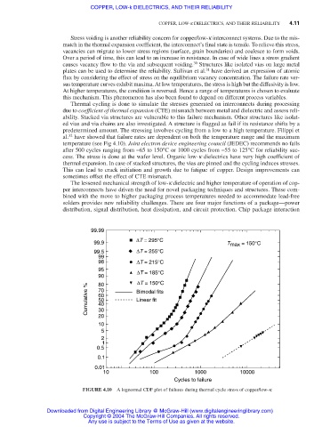
Thermal cycling is done to simulate the stresses generated on interconnects during processing
due to coefficient of thermal expansion (CTE) mismatch between metal and dielectric and assess reli-
ability. Stacked via structures are vulnerable to this failure mechanism. Other structures like isolat-
ed vias and via chains are also investigated. A structure is flagged as fail if its resistance shifts by a
predetermined amount. The stressing involves cycling from a low to a high temperature. Filippi et
32
al. have showed that failure rates are dependent on both the temperature range and the maximum
temperature (see Fig 4.10). Joint electron device engineering council (JEDEC) recommends no fails
after 500 cycles ranging from −65 to 150°C or 1000 cycles from −55 to 125°C for reliability suc-
cess. The stress is done at the wafer level. Organic low-k dielectrics have very high coefficient of
thermal expansion. In case of stacked structures, the vias are pinned and the cycling induces stresses.
This can lead to crack initiation and growth due to fatigue of copper. Design improvements can
sometimes offset the effect of CTE mismatch.
The lessened mechanical strength of low-k dielectric and higher temperature of operation of cop-
per interconnects have driven the need for novel packaging techniques and structures. These com-
bined with the move to higher packaging process temperatures needed to accommodate lead-free
solders provides new reliability challenges. There are four major functions of a package—power
distribution, signal distribution, heat dissipation, and circuit protection. Chip package interaction
99.99
∆T = 295°C
99.9 T max = 150°C
99.5 ∆T = 255°C
99
98 ∆T = 215°C
95 ∆T = 185°C
90 ∆T = 150°C
80
Cumulative % 70 Bimodal fits
60
50
Linear fit
40
30
20
10
5
2
1
0.5
0.1
0.01
10 100 1000 10000
Cycles to failure
FIGURE 4.10 A lognormal CDF plot of failures during thermal cycle stress of copper/low-κ.
Downloaded from Digital Engineering Library @ McGraw-Hill (www.digitalengineeringlibrary.com)
Copyright © 2004 The McGraw-Hill Companies. All rights reserved.
Any use is subject to the Terms of Use as given at the website.