Page 53 - Semiconductor Manufacturing Handbook
P. 53

Geng(SMH)_CH05.qxd  04/04/2005  19:37  Page 5.2


                                          FUNDAMENTALS OF SILICIDE FORMATION ON Si

                   5.2  SEMICONDUCTOR FUNDAMENTALS AND BASIC MATERIALS

                   5.1.2 MOS Device—RC Delay and Speed at the Gate
                   and Interconnection Level

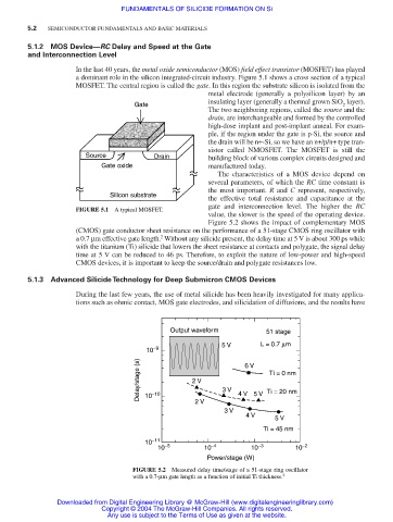
                               In the last 40 years, the metal oxide semiconductor (MOS) field effect transistor (MOSFET) has played
                               a dominant role in the silicon integrated-circuit industry. Figure 5.1 shows a cross section of a typical
                               MOSFET. The central region is called the gate. In this region the substrate silicon is isolated from the
                                                                metal electrode (generally a polysilicon layer) by an
                                                                insulating layer (generally a thermal grown SiO layer).
                                              Gate                                               2
                                                                The two neighboring regions, called the source and the
                                                                drain, are interchangeable and formed by the controlled
                                                                high-dose implant and post-implant anneal. For exam-
                                                                ple, if the region under the gate is p-Si, the source and
                                                                the drain will be n+-Si, so we have an n+/p/n+ type tran-
                                                                sistor called NMOSFET.  The MOSFET is still the
                                 Source           Drain         building block of various complex circuits designed and
                                     Gate oxide                 manufactured today.
                                                                  The characteristics of a MOS device depend on
                                                                several parameters, of which the RC time constant is
                                                                the most important. R and C represent, respectively,
                                       Silicon substrate
                                                                the effective total resistance and capacitance at the
                                                                gate and interconnection level.  The higher the  RC
                               FIGURE 5.1  A typical MOSFET.
                                                                value, the slower is the speed of the operating device.
                                                                Figure 5.2 shows the impact of complementary MOS
                               (CMOS) gate conductor sheet resistance on the performance of a 51-stage CMOS ring oscillator with
                                                    2
                               a 0.7 µm effective gate length. Without any silicide present, the delay time at 5 V is about 300 ps while
                               with the titanium (Ti) silicide that lowers the sheet resistance at contacts and polygate, the signal delay
                               time at 5 V can be reduced to 46 ps. Therefore, to exploit the nature of low-power and high-speed
                               CMOS devices, it is important to keep the source/drain and polygate resistances low.
                   5.1.3 Advanced Silicide Technology for Deep Submicron CMOS Devices

                               During the last few years, the use of metal silicide has been heavily investigated for many applica-
                               tions such as ohmic contact, MOS gate electrodes, and silicidation of diffusions, and the results have


                                                      Output waveform         51 stage

                                                                   5 V       L = 0.7 µm
                                                10 −9
                                               Delay/stage (s)  −10  2 V  3 V  4 V 6 V 5 V  Ti = 20 nm
                                                                               Ti = 0 nm

                                                10
                                                             2 V
                                                                    3 V
                                                                         4 V
                                                                                 5 V
                                                                              Ti = 45 nm
                                                10 −11
                                                   10 −5       10 −4       10 −3      10 −2
                                                                Power/stage (W)
                                             FIGURE 5.2  Measured delay time/stage of a 51-stage ring oscillator
                                             with a 0.7-µm gate length as a function of initial Ti thickness. 2


                          Downloaded from Digital Engineering Library @ McGraw-Hill (www.digitalengineeringlibrary.com)
                                     Copyright © 2004 The McGraw-Hill Companies. All rights reserved.
                                       Any use is subject to the Terms of Use as given at the website.
   48   49   50   51   52   53   54   55   56   57   58