
Page 54 - Semiconductor Manufacturing Handbook
P. 54
Geng(SMH)_CH05.qxd 04/04/2005 19:37 Page 5.3
FUNDAMENTALS OF SILICIDE FORMATION ON Si
FUNDAMENTALS OF SILICIDE FORMATION ON Si 5.3
been very exciting. Silicides of titanium, cobalt, nickel, platinum, tungsten, molybdenum, tantalum,
and other metals have reasonable good compatibility with IC fabrication technology for one or more
applications mentioned earlier. They have fairly high conductivity and resistance to electromigration,
can make low resistance and reliable contacts to shallow p-n junctions, and can withstand the chem-
icals normally encountered during the fabrication process.
However, to incorporate the silicides in a microelectronics structure, many problems must be
understood for the proper functioning of the device. Important issues are that the silicides involve non-
homogeneous materials and often contain a secondary and metastable phase. Equally important is the
presence of adjoining layers and the interfaces between them, and the role they play in the different
processes and mechanisms. As the semiconductor structures get smaller, these adjoining layers and
interfaces can dominate the various phenomena in interconnect processing. In addition, even the inter-
faces themselves can act as separate phases and greatly affect the film properties and processing.
For the silicide process, low-resistivity silicide layers are obtained by depositing the silicide
directly, or by depositing the metal on silicon and reacting the materials to form the silicide. In all
of these cases a detailed knowledge of the formation techniques, properties of as-formed films, and
changes during the subsequent processing is absolutely necessary.
5.2 WHAT ARE THE FUNDAMENTALS OF SILICIDATION ON Si?
5.2.1 Properties
The resistivity of the silicide is the most important criterion for considering metallization in inte-
grated circuits. Investigations of various metal-silicon systems have resulted in silicide resistivities
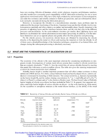
that are routinely obtainable. 3,4 Table 5.1 lists the resistivities of various silicides formed by reacting
thin metal film with mono or polycrystalline silicon. The table also gives the sintering temperatures
at which the lowest resistivities were obtained.
Schottky barrier height is another important parameter that will affect contact resistance in deep
submicron CMOS devices. For ohmic contact between metal and heavily doped silicon, current con-
duction is dominated by tunneling or field emission. The contact resistivity r depends exponentially
c
10
1/2
on the barrier height Φ and the surface doping concentration N : r exp[4pΦ /qh (m*e /N ) ],
B d c B si d
where h is Planck’s constant and m* is the electron effective mass. The best known value of Schottky
barrier heights of silicide on n-silicon has been included in Table 5.1. In general, four apparent vari-
ables control the barrier heights of various silicides on silicon—(a) the work function f of the metal,
M
(b) the crystalline or amorphous structure at the metal-silicon interface, (c) the ability of the metal
TABLE 5.1 Resistivity of Various Silicides and Schottky Barrier Value of Silicide on n-Silicon
Self-aligned Resistivity Useful Φ
B
Silicide reaction temp. (°C) (µΩ-cm) temperature (°C) (eV)
TiSi 625–675 a <950 0.60 5
2
850–900 b 13–16
CoSi 400–540 a <900 0.64 5
2
700–800 b 18–20
NiSi 400–650 ~50 <700 0.65 6
Pd Si 175–450 30–35 0.71 7
2
PtSi 400–600 28–35 <800 0.88 8
+
0.21 for p -type
WSi 690–740 ~70 0.65 5
2
MoSi 850 90~100 0.55 9
2
a
First anneal followed by the selective metal etch.
b
Second anneal to form the low-resistivity silicide.
Downloaded from Digital Engineering Library @ McGraw-Hill (www.digitalengineeringlibrary.com)
Copyright © 2004 The McGraw-Hill Companies. All rights reserved.
Any use is subject to the Terms of Use as given at the website.