
Page 59 - Semiconductor Manufacturing Handbook
P. 59
Geng(SMH)_CH05.qxd 04/04/2005 19:37 Page 5.8
FUNDAMENTALS OF SILICIDE FORMATION ON Si
5.8 SEMICONDUCTOR FUNDAMENTALS AND BASIC MATERIALS
wafers by low-pressure chemical vapor deposition (LPCVD) has been investigated as an alternative
choice for small dimensional devices. In the CVD process, the silicide thickness is no longer limit-
ed by the shallow source/drain junction, and substrate doping does not have a strong effect on sili-
cide growth. More important, the sheet resistance is not affected by polysilicon line-width because
the formation of the C54 phase occurs during deposition. One remaining issue of this technology is
the silicide/Si-specific contact resistivity.
5.3.2 Nanosilicide Formation
33
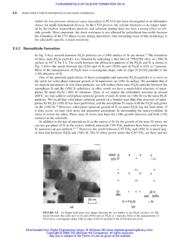
In Fig. 5.4(a), several nanosize Pd Si particles on a (100) surface of Si are shown. The formation
2
of these nano-Pd Si particles was obtained by annealing a thin film of 75Pd25Er alloy on (100) Si
2
surface at 347°C for 1 h. The misfit between the diffraction patterns of the Pd Si and Si is shown in
2
Fig. 5.4(b)—the misfit between the (220) spot of Si and (3030) spot of Pd Si is 0.03 or 3 percent.
2
Most of the nanoparticles of Pd Si have a rectangular shape with its edge of [0110] parallel to the
2
[110] direction of Si.
One of the potential applications of these rectangular and nanosize Pd Si particles is to serve as
2
the seeds for solid-phase epitaxial growth of Si nanowires on (100) Si surface. We postulate that if
we deposit amorphous Si over these particles, we will embed these nano-Pd Si particles between the
2
amorphous Si and the (100) Si substrates, in other words we have a sandwiched structure of amor-
phous Si/ nano-Pd Si/ (100) Si substrate. Then, if we anneal the embedded structure at around
2
400°C, we may achieve solid-phase epitaxial growth of nano-Si wires on (100) Si via the nano-Pd Si
2
particles. We recall that solid-phase epitaxial growth of a blanket-type thin film structure of amor-
phous Si/ Pd Si/ (100) Si has been performed, and the amorphous Si reacts with the Pd Si and grows
2 2
34
on the (100) Si. However, solid-phase epitaxial growth of Si on nano-Pd Si has not been done. If
2
it does occur, we may etch away the unreacted amorphous Si surrounding the nanocrystalline Si
wires to reveal the wires. These nano Si wires may have the (100) growth direction and with (110)
surfaces as the sidewalls.
In addition to the use of amorphous Si as the source of Si for the growth of the nano-Si wires, we
can use gas phase of Si as the source. Indeed, nanoscale C49-TiSi particles have been used to grow
2
Si nanowires in gas ambient. 35–37 However, the misfit between C49 TiSi and (100) Si is much larg-
2
er than that between Pd Si and (100) Si. The Si wires grown under the C49 TiSi are bent and not
2 2
0002−
220−× ×
000 –
220 3030
50 nm
Pd Si × Si
2
(a) (b)
FIGURE 5.4 (a) Bright-field plan-view image showing the two habits of the Pd Si crystals. (b) The
2
misfit between the (220) spot of Si and (3030) spot of Pd Si is 3 percent. Most of the nanoparticles of
2
Pd Si have a rectangular shape with its edge of [0110] parallel to the [110] direction of Si.
2
Downloaded from Digital Engineering Library @ McGraw-Hill (www.digitalengineeringlibrary.com)
Copyright © 2004 The McGraw-Hill Companies. All rights reserved.
Any use is subject to the Terms of Use as given at the website.