
Page 58 - Semiconductor Manufacturing Handbook
P. 58
Geng(SMH)_CH05.qxd 04/04/2005 19:37 Page 5.7
FUNDAMENTALS OF SILICIDE FORMATION ON Si
FUNDAMENTALS OF SILICIDE FORMATION ON Si 5.7
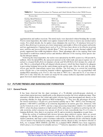
TABLE 5.7 Fabrication Procedure for Titanium and Cobalt Silicide Films in the CMOS Process
Process flow TiSi CoSi
2 2
Starting Metal/Thickness Ti/35 nm Co/32 nm
Capping Layer/Thickness TiN/15 nm Ti/20 nm
Metal Deposition Method Sputter or evaporation Sputter or evaporation
First RTA 675°C/120 s 475°C/3 min
Select Wet Etch 4:1, 120°C/10 min 1:1:1, 65°C/1 min
H SO :H O NH OH:H O :H O
2 4 2 2 4 2 2 2
Second RTA 850°C/1 min 700°C/1 min
agglomeration and surface reactions. The metal stacks were deposited without breaking the vacuum.
Prior to metal deposition, the wafers were sputter cleaned with Ar ions to remove any residual native
oxides. For cobalt silicide, the Ar sputter clean eliminates the need for a Ti interlayer between Co
and Si, thus allowing it to process at a lower temperature and results in films with greater uniformity
and less agglomeration. Capping layers such as Ti or TiN have been shown to be effective in giving
28
more uniform and lower-resistivity silicide films. They also lead to greater thermal stability and
greatly suppressed line-width degradation effects. These advantages due to the capping films were
speculated to result from reduced surface and interface diffusion of the reacting metal species dur-
ing the nitrogen anneal.
Following the metal deposition, the wafers were annealed by the RTA system in a 100 percent N
2
ambient. After the initial RTA, the unreacted material on the field oxide and spacer regions was wet
etched in a heated H SO :H O for titanium silicide and NH OH:H O :H O mixture for cobalt sili-
2 4 2 2 4 2 2 2
cide. This is a critical part of the self-aligned silicide process, which has been found to be adequate
in preventing bridging between the source/drain region and the gate. After the etch, only the poly-
silicon gate and the source/drain region have silicides. The final step is to convert the remaining
active silicide into a low-resistivity material without agglomeration. This was accomplished with
another RTA annealing cycle. For Co, this was done at 700°C for 1 min and for Ti, it was done at
850°C for 1 min. After this, the wafers are ready for the contact dielectric deposition and the subse-
quent first-level metal-interconnect processing.
5.3 FUTURE TRENDS AND NANOSILICIDE FORMATION
5.3.1 General Trends
It has been observed that the sheet resistance of a Ti-silicided polysilicon-gate electrode or
source/drain region increases significantly as the dimension reaches the lower submicron range. Thus
alternative silicide choices like cobalt and nickel silicides have been investigated and chosen as the
promising silicides for deep submicron MOS technologies. 29,30 They have the advantages of having
the lowest resistivities (~20 µΩ-cm), good thermal stability (up to 700 ~ 900°C), low forming tem-
perature (~400–600°C) and little or no resistivity degradation on narrow gate lines. Moreover, NiSi
can be formed at as low as 450°C, and has a large processing temperature window. It is stable up to
650°C, where the phase transition to high resistive NiSi takes place. In addition to achieving low sili-
2
cide resistivity, nickel consumes less amount of silicon to form monosilicide than Ti or Co does in
forming disilicide. Also, there is no reaction with N and no resistivity degradation on gate lines.
2
When the scaling of traditional bulk devices becomes deep submicro regime, there are several
challenges for silicide process development—well-controlled thin film silicide is essential due to
shallow junctions; and large contact resistance induced by conventional silicide with barrier height
~0.6 eV needs to be decreased by using an alternative silicide. Based on this, low-barrier silicides of
ErSi for n-channel MOS (NMOS) and PtSi for p-channel MOS (PMOS) have been suggested,
2
which attract a lot of interest for ultrathin devices. 31,32 Selective deposition of the silicide on bulk Si
Downloaded from Digital Engineering Library @ McGraw-Hill (www.digitalengineeringlibrary.com)
Copyright © 2004 The McGraw-Hill Companies. All rights reserved.
Any use is subject to the Terms of Use as given at the website.