
Page 57 - Semiconductor Manufacturing Handbook
P. 57
Geng(SMH)_CH05.qxd 04/04/2005 19:37 Page 5.6
FUNDAMENTALS OF SILICIDE FORMATION ON Si
5.6 SEMICONDUCTOR FUNDAMENTALS AND BASIC MATERIALS
TABLE 5.6 Results of the Growth Kinetics of Silicide Thin Films: Silicide Formed,
Range of Formation, Activation Energy, Dominant Diffusing Species (DDS), and Kinetics
Time
Silicide Tf (°C) Q (eV) 1 DDS dependence
TiSi 550–650 2.5 Si t 1/2
2
575–750 2.5
Co Si 350–500 1.5 Co t 1/2
2
CoSi 400–550 1.75 Si t 1/2
CoSi 405–500 2.3 Co
2
NiSi 250–400 1.4 Ni t
Pd Si 175–450 1.4 Pd-Si t 1/2
2
PtSi 300–540 1.5 Pt-Si? t 1/2
WSi 850–1100 3, 2.2 Si t, t 1/2
2
MoSi 474–550 3.2, 2.4 t, t 1/2
2
850–1100 2.2 Si
first, then a second high-temperature anneal is needed to convert C49 to low resistivity phase C54.
Similar information has been obtained for cobalt silicide. Table 5.6 summarizes the results of the
growth and transformation of various silicides at different temperatures. In most cases a t 1/2 depen-
dence of the phase growth has been found, indicating a diffusion-limited growth, where the thick-
2
ness of the silicide layer formed in time t is given by X = Dt. In some cases a linear dependence on
time was found, suggesting an interface rate-controlled interaction and the thickness is given by X =
Dt, where D represents interface diffusivities during silicide formation. These data are quite useful
for practical applications—reacted silicide thickness at the specific temperature and time can be cal-
culated by using these data.
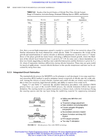
5.2.3 Integrated-Circuit Fabrication
The standard silicide process for MOSFETs on Si substrates is well developed. A two-step rapid ther-
mal annealing (RTA) method is used to minimize lateral overgrowth of silicide onto the oxide side-
wall. Among the choices of metal silicides, titanium and cobalt silicides are widely used in industry
due to their low resistivity, high thermal stability, and ability to remove from oxide on Si.
Figure 5.3 and Table 5.7 represent the detailed fabrication procedures with standard CMOS
process flow—as a part of the overall CMOS process, the silicide formation follows the spacer
definition. The starting metal was sputter deposited as a bilayer stack, with the bottom layer being
the reacting species and the top layer being the stabilizing material for suppressing unwanted
Gate ♣ Active area definition and
LOCOS
Source Drain
♣ Threshold voltage adjustment
Substrate ♣ Gate oxidation and polydeposition
♣ E-beam polygate lithography
and polyetch
♣ Source/drain extension implant
Silicide Gate Silicide ♣ Spacer formation and deep S/D
implant
♣ RTA dopant activation
Substrate ♣ Two step Ti silicidation
FIGURE 5.3 Silicide process flow with CMOS technology.
Downloaded from Digital Engineering Library @ McGraw-Hill (www.digitalengineeringlibrary.com)
Copyright © 2004 The McGraw-Hill Companies. All rights reserved.
Any use is subject to the Terms of Use as given at the website.