
Page 64 - Semiconductor Manufacturing Handbook
P. 64
Geng(SMH)_CH06.qxd 04/04/2005 19:37 Page 6.3
PLASMA PROCESS CONTROL
PLASMA PROCESS CONTROL 6.3
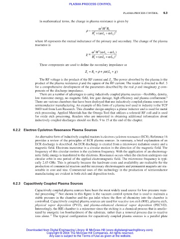
In mathematical terms, the change in plasma resistance is given by
2
2
r = w MR 2
R 2 2 + ( w L e + w L ) 2
2
where M represents the mutual inductance of the primary and secondary. The change of the plasma
reactance is
2
2
c = w M ( w L e + w L )
2
R 2 + ( w L + w L ) 2
2 e 2
These components are used to define the secondary impedance as
Z = R + + jw( L + c)
r
s
o
o
The RF voltage is the product of the RF current and Z . The power absorbed by the plasma is the
s
product of the plasma resistance r and the square of the RF current. The reader is directed to Ref. 3
for a comprehensive development of the parameters described by the real r and imaginary c com-
ponents of the discharge impedance.
There are a number of advantages to using inductively coupled plasma sources—flexibility, density,
low transverse energy, no magnetic field, low gate damage, high efficiency and plasma confinement. 8
There are various chambers that have been deployed that use inductively coupled plasma sources for
semiconductor manufacturing. An example of this form of a plasma tool used in industry is the TCP
9600 tool from Lam Research. This chamber design employs a planar inductor and is used for metal
etch processing. Applied Materials has the Omega Tool that utilizes a solenoid RF coil and is used
for oxide etch processing. Readers who are interested in obtaining additional information about
inductively coupled discharges should see Refs. 9 to 15 at the end of the chapter.
6.2.2 Electron Cyclotron Resonance Plasma Sources
An alternative form of inductively coupled reactors is electron cyclotron resonance (ECR). Reference 16
provides a review of the principles of ECR plasma sources. In summary, a brief explanation of an
ECR discharge is described. An ECR discharge is created from a microwave radiation source and a
magnetic field. Electrons transverse in a circular motion in the direction of the magnetic field. The
frequency of this circular motion is the cyclotron frequency. With the application of an electromag-
netic field, energy is transferred to the electrons. Resonance occurs when the electron undergoes one
circular orbit in one period of the applied electromagnetic field. The microwave frequency is typi-
cally 2.45 GHz. This is primarily because the hardware costs and availability are realizable for the
production of commercial reactors and the necessary electromagnets and permanent magnets are rea-
sonable in cost and size. Commercial uses of this technology in the production of semiconductor
manufacturing are evident in both etch and deposition tools.
6.2.3 Capacitively Coupled Plasma Sources
Capacitively coupled plasma sources have been the most widely used source for low-pressure mate-
17
rial processing. Not shown in this figure is the vacuum control system that is used to maintain a
stable pressure in the chamber and the gas inlet where the flow of chemistry into the chamber is
controlled. Capacitively coupled plasma sources are used for reactive ion etch (RIE), plasma etch,
physical vapor deposition (PVD), and plasma-enhanced chemical vapor deposition (PECVD).
Interestingly, the RIE chamber is a misnomer since the etching is a chemical process that is amelio-
rated by energetic ion bombardment of the substrate, rather than a removal process due to reactive
17
ions alone. The typical configuration for capacitively coupled plasma sources is a parallel plate
Downloaded from Digital Engineering Library @ McGraw-Hill (www.digitalengineeringlibrary.com)
Copyright © 2004 The McGraw-Hill Companies. All rights reserved.
Any use is subject to the Terms of Use as given at the website.