
Page 67 - Semiconductor Manufacturing Handbook
P. 67
Geng(SMH)_CH06.qxd 04/04/2005 19:37 Page 6.6
PLASMA PROCESS CONTROL
6.6 SEMICONDUCTOR FUNDAMENTALS AND BASIC MATERIALS
The plasma resistance and capacitance are obtained from
R = R + R
s b
s[
+
2
)
C 1 (w C R ]
C = s s
(w CR ) 2
s s
Capacitively coupled plasmas have the disadvantage of high sheath voltages with low ion density
and high ion bombarding energy. The ion bombarding energy cannot be controlled independent of
17
the ion energy. The addition of a magnetron to the capacitively coupled plasma system is an attempt
to achieve these goals. The magnetically enhanced reactive ion etcher (MERIE) is described in the
section that follows.
6.2.4 Magnetic Plasma Sources
Magnetrons are also used to ameliorate plasma or ion density and uniformity for the production of
semiconductor devices. Typically, they are found in sputtering systems that deposit metal (aluminum
or copper) onto a target. Reference 20 is explicitly used here as a source to describe the physical uti-
lization and features of using a magnetron. The efficacy of using a magnetron is related to the efficiency
between power density and etch rate. Only the ion energy across the surface of the wafer is useable for
etching. This results in a volume of unusable ion energy. Increasing the power density is generally not
a viable solution because with the increase in power, there is a proportional increase in heat and loss.
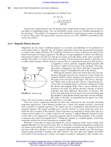
A magnetron is used to generate a magnetic field in parallel with
the wafer to confine the ion energy of the discharge. This mag-
Electric Electron netic field is orthogonal to the electric field that is generated by
field path the plasma. Figure 6.5 illustrates the path of the electron.
Although the magnetic field is not shown due to the 3D visu-
alization challenges posed by the interaction of these fields, the
magnetic field for a dipole magnet can be imagined to travel into
r
the paper at the solid point in this figure. The electric and mag-
netic fields create an electron drift velocity component that tra-
verses with a closed path radius in a direction orthogonal to both
the electric and magnetic fields. This is shown with the arrow
pointing to the right. The drifting electrons impinge on neutral
molecules and cause additional dissociation of electrons. The
FIGURE 6.5 Electron path. closed-loop path of the electron results in an electron storage ring
that produces a high plasma density and limits electron mobility.
The radius of the path r is proportional to the square root of the
energy. The electron path is typically referred to as cycloidal.
There are several commercial methods that have been employed for the previously described
magnetron applications. Tokyo Electron Limited uses a dipole ring magnet assembly constructed
21
with a plurality of magnetic segments. The dipole ring has a nonmagnetic material between each
magnetic segment. The magnet assembly uses a circular rotation on a track around the center axis
about the outer periphery of the chamber. Tylan Corporation accomplished a similar effect that uses
20
a linear motion in place of a circular rotation for the magnets. Applied Materials obtained similar
results with a novel approach of using electromagnets spaced around the periphery of the chamber
22
to generate and control the magnetic field. Pulsing the magnets in a periodic fashion controls the
magnitude and direction of the instantaneous magnetic field.
Reference 23 provides an elegant description of a recent magnetron sputter reactor design from
Applied Materials. For this reactor design, Ref. 24 elaborates on the three magnetrons contained in
this sputter reactor design. There are two circular ring magnet assemblies that are located on the roof
and inner wall of the chamber vessel. These magnets rotate about the chamber axis. The third ring-
shaped magnet assembly is located at the outer sidewall. The inner and outer magnet assemblies
are parallel to the chamber axis and the roof magnet assembly is orthogonal to the chamber axis.
Downloaded from Digital Engineering Library @ McGraw-Hill (www.digitalengineeringlibrary.com)
Copyright © 2004 The McGraw-Hill Companies. All rights reserved.
Any use is subject to the Terms of Use as given at the website.