
Page 65 - Semiconductor Manufacturing Handbook
P. 65
Geng(SMH)_CH06.qxd 04/04/2005 19:37 Page 6.4
PLASMA PROCESS CONTROL
6.4 SEMICONDUCTOR FUNDAMENTALS AND BASIC MATERIALS
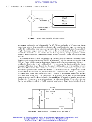
Sheath
RF source
Electrodes Plasma
Sheath
Chamber under
vacuum
FIGURE 6.3 Physical model of a parallel plate plasma source. 17
arrangement of electrodes and is illustrated in Fig. 6.3. With the application of RF energy, the plasma
is developed between the upper and lower electrodes. For simplification, the upper electrode is pow-
ered in this model and the lower electrode is grounded. Some industrial applications for capacitively
coupled discharges employ a second RF source at the lower electrode. A sheath is generated
between the electrodes and the plasma. The sheath is a positively charged layer that confines
electrons. The electrons are confined because the electric field in the sheath is directed from the
plasma. 17
The industry standardized the parallel plate configuration and referred to this chamber design as
the Gaseous Electronics Conference (GEC) RF reference cell. It is also commonly referred to as the
18
GEC cell. Figure 6.4 illustrates the circuit model for this parallel plate chamber design. Reference 19
is utilized to describe the circuit model and Ref. 17 to correspond the circuit model to the plasma
parameters. The shunt circuit elements (L , C , and R ) will be addressed in the matching network
s
s
s
discussion of this chapter. The circuit model includes the parasitic elements that are present in the
powered and ground electrodes and in the chamber wall. Note that sometimes the powered electrode
is referred to as the anode and the grounded electrode is referred to as the cathode. C PE is the para-
sitic capacitance for the powered electrode and is attributed to the insulator between the powered
electrode and the ground shield. The transmission line that powers the electrode is represented by the
series elements L and R . Typical chamber designs will have RF metrology installed in situ before
PE
PE
the electrode. C represents the shunt capacitance that is introduced by the RF metrology. L PE and
M
R may also address the effects of the RF metrology. Analogous to the powered electrode, elements
PE
L PE
R PE
L S I PE R GE
V RF C M C PE C GE
C S L GE
R S
L W
FIGURE 6.4 Electrical model of a capacitively coupled plasma source. 19
Downloaded from Digital Engineering Library @ McGraw-Hill (www.digitalengineeringlibrary.com)
Copyright © 2004 The McGraw-Hill Companies. All rights reserved.
Any use is subject to the Terms of Use as given at the website.