
Page 69 - Semiconductor Manufacturing Handbook
P. 69
Geng(SMH)_CH06.qxd 04/04/2005 19:37 Page 6.8
PLASMA PROCESS CONTROL
6.8 SEMICONDUCTOR FUNDAMENTALS AND BASIC MATERIALS
C
L
L L L L
C C C C
T network L networks PI network
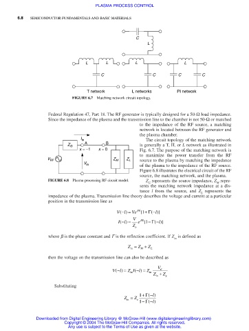
FIGURE 6.7 Matching network circuit topology.
Federal Regulation 47, Part 18. The RF generator is typically designed for a 50-Ω load impedance.
Since the impedance of the plasma and the transmission line to the chamber is not 50-Ω or matched
to the impedance of the RF source, a matching
network is located between the RF generator and
the plasma chamber.
I in The circuit topology of the matching network
A B
Z G is generally a T, Π, or L network as illustrated in
x = −1 x = 0 Fig. 6.7. The purpose of the matching network is
to maximize the power transfer from the RF
V RF Z M Z L source to the plasma by matching the impedance
V in of the plasma to the impedance of the RF source.
Figure 6.8 illustrates the electrical circuit of the RF
source, the matching network, and the plasma.
FIGURE 6.8 Plasma processing RF circuit model. Z represents the source impedance, Z repre-
G M
sents the matching network impedance at a dis-
tance l from the source, and Z represents the
L
impedance of the plasma. Transmission line theory describes the voltage and current at a particular
position in the transmission line as
Β
V()−= Ve [ + Γ ()]
−
jl
1
l
l
Β
I()−= V e [ − Γ1 ()]
−
jl
l
l
Z o
where β is the phase constant and Γ is the reflection coefficient. If Z is defined as
in
Z = Z + Z
in M L
then the voltage on the transmission line can also be described as
V()−= Z I()−= Z V rf
l
l
in
Z + Z g
in
in
Substituting
l −
Z = Z 1 + Γ()
o
l −
in
1 − Γ()
Downloaded from Digital Engineering Library @ McGraw-Hill (www.digitalengineeringlibrary.com)
Copyright © 2004 The McGraw-Hill Companies. All rights reserved.
Any use is subject to the Terms of Use as given at the website.