
Page 73 - Semiconductor Manufacturing Handbook
P. 73
Geng(SMH)_CH06.qxd 04/04/2005 19:37 Page 6.12
PLASMA PROCESS CONTROL
6.12 SEMICONDUCTOR FUNDAMENTALS AND BASIC MATERIALS
and a silver-plated copper inner conductor. The geometry of the inner conductor is square with cham-
fered corners. The material of the dielectric spacer is boron nitride. The boron-nitride dielectric and the
silver-plated inner conductor are designed specifically to permit the higher operating current at higher
frequencies. The square shaft of the conductor has demonstrated improved coupling for increased
signal-to-noise ratio. The square shaft also increases the surface area for optimal heat transfer from the
inner conductor to the body of the probe. These design features have enhanced the absolute and unit-
to-unit repeatability accuracy. They also permit the use of the probe in high frequencies (greater than
13.56 MHz), high-current applications without performance degradation at low frequencies, and power
applications. The sensor comprises voltage and current pick-up assemblies. The voltage pick-up assem-
bly converts the time-varying electric field created on the inner conductor to a small voltage signal rep-
resentative of the line voltage(s). The current pick-up assembly converts the time-varying magnetic
field created on the inner conductor to a small voltage signal representative of the line current(s). These
voltage and current signals are connected to an associated analysis module.
A feature-rich signal processing architecture of an analysis module for an RF impedance/power
50
sensor is described. One of the significant advantages of this signal-processing architecture is its
ability to autonomously track multiple RF sources. This is accomplished through a high-speed sam-
pling and digital processing unit. The signal-processing architecture is analogous to phase lock loop;
however in this case the implementation is in the form of analog and digital electronics.
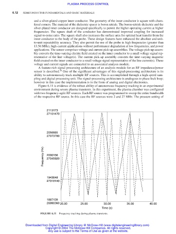
Figure 6.11 is evidence of the robust ability of autonomous frequency tracking in an experimental
environment during severe plasma transients. In this experiment, the plasma chamber was configured
with two frequency-agile RF sources. Each RF source was programmed to sweep the entire bandwidth
of the respective RF source. In this case the RF sources were 2 and 27 MHz. The pressure setting of
2113173
27101470
2056665
27073700
Frequency (Hz) 2000156
27045920
1943648
27018140
1887139
26990360 20.00 25.00 30.00 35.00 40.00
Time (s)
FIGURE 6.11 Frequency tracking during plasma transients.
Downloaded from Digital Engineering Library @ McGraw-Hill (www.digitalengineeringlibrary.com)
Copyright © 2004 The McGraw-Hill Companies. All rights reserved.
Any use is subject to the Terms of Use as given at the website.