
Page 47 - Semiconductor Manufacturing Handbook
P. 47
Geng(SMH)_CH04.qxd 04/04/2005 19:36 Page 4.10
COPPER, LOW-k DIELECTRICS, AND THEIR RELIABILITY
4.10 SEMICONDUCTOR FUNDAMENTALS AND BASIC MATERIALS
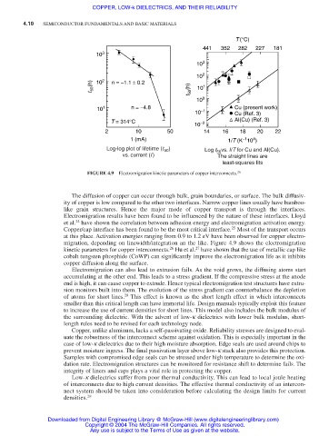
T (°C)
441 352 282 227 181
10 3
10 3
10 2
2
t 50 (h) 10 n = −1.1 ± 0.2 t 50 (h) 10 1
10 0
10 1 n = −4.8 Cu (present work)
10 −1 Cu (Ref. 3)
T = 314°C −2 Al(Cu) (Ref. 3)
10
2 10 50 14 16 18 20 22
1 (mA) 1/T (K 10 )
4
−1
Log-log plot of lifetime (t ) Log t vs. I/T for Cu and Al(Cu).
50
50
vs. current (I) The straight lines are
least-squares fits
FIGURE 4.9 Electromigration kinetic parameters of copper interconnects. 26
The diffusion of copper can occur through bulk, grain boundaries, or surface. The bulk diffusiv-
ity of copper is low compared to the other two interfaces. Narrow copper lines usually have bamboo-
like grain structures. Hence the major mode of copper transport is through the interfaces.
Electromigration results have been found to be influenced by the nature of these interfaces. Lloyd
24
et al. have shown the correlation between adhesion energy and electromigration activation energy.
25
Copper/cap interface has been found to be the most critical interface. Most of the transport occurs
at this place. Activation energies ranging from 0.9 to 1.2 eV have been observed for copper electro-
migration, depending on linewidth/integration an the like. Figure 4.9 shows the electromigration
27
26
kinetic parameters for copper interconnects. Hu et al. have shown that the use of metallic cap like
cobalt tungsten phosphide (CoWP) can significantly improve the electromigration life as it inhibits
copper diffusion along the surface.
Electromigration can also lead to extrusion fails. As the void grows, the diffusing atoms start
accumulating at the other end. This leads to a stress gradient. If the compressive stress at the anode
end is high, it can cause copper to extrude. Hence typical electromigration test structures have extru-
sion monitors built into them. The evolution of the stress gradient can counterbalance the depletion
of atoms for short lines. 28 This effect is known as the short length effect in which interconnects
smaller than this critical length can have immortal life. Design manuals typically exploit this feature
to increase the use of current densities for short lines. This model also includes the bulk modulus of
the surrounding dielectric. With the advent of low-k dielectrics with lower bulk modulus, short-
length rules need to be revised for each technology node.
Copper, unlike aluminum, lacks a self-passivating oxide. Reliability stresses are designed to eval-
uate the robustness of the interconnect scheme against oxidation. This is especially important in the
case of low-k dielectrics due to their high moisture absorption. Edge seals are used around chips to
prevent moisture ingress. The final passivation layer above low-k stack also provides this protection.
Samples with compromised edge seals can be stressed under high temperature to determine the oxi-
dation rate. Electromigration structures can be monitored for resistance shift to determine fails. The
integrity of liners and caps plays a vital role in protecting the copper.
Low-k dielectrics suffer from poor thermal conductivity. This can lead to local joule heating
of interconnects due to high current densities. The effective thermal conductivity of an intercon-
nect system should be taken into consideration before calculating the design limits for current
densities. 29
Downloaded from Digital Engineering Library @ McGraw-Hill (www.digitalengineeringlibrary.com)
Copyright © 2004 The McGraw-Hill Companies. All rights reserved.
Any use is subject to the Terms of Use as given at the website.