
Page 42 - Semiconductor Manufacturing Handbook
P. 42
Geng(SMH)_CH04.qxd 04/04/2005 19:36 Page 4.5
COPPER, LOW-k DIELECTRICS, AND THEIR RELIABILITY
COPPER, LOW-κ DIELECTRICS, AND THEIR RELIABILITY 4.5
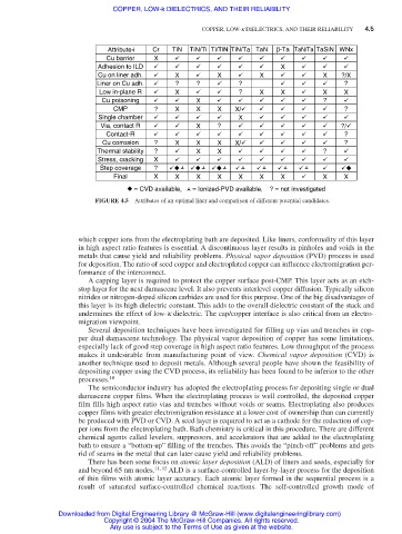
Attribute Cr TiN TiN/Ti Ti/TiN TiN/Ta TaN β-Ta TaN/Ta TaSiN WNx
Cu barrier X
Adhesion to ILD X
Cu on liner adh. X X X X ?/X
Liner on Cu adh. ? ? ? ?
Low in-plane R X ? X X X X
Cu poisoning X ?
CMP ? X X X ?
Single chamber X
Via, contact R X ?
Contact-R ?
Cu corrosion ? X X X ?
Thermal stability ? X X ?
Stress, cracking X
Step coverage ?
Final X X X X X X X X X
= CVD available, = Ionized-PVD available, ? = not investigated
FIGURE 4.5 Attributes of an optimal liner and comparison of different potential candidates.
which copper ions from the electroplating bath are deposited. Like liners, conformality of this layer
in high aspect ratio features is essential. A discontinuous layer results in pinholes and voids in the
metals that cause yield and reliability problems. Physical vapor deposition (PVD) process is used
for deposition. The ratio of seed copper and electroplated copper can influence electromigration per-
formance of the interconnect.
A capping layer is required to protect the copper surface post-CMP. This layer acts as an etch-
stop layer for the next damascene level. It also prevents interlevel copper diffusion. Typically silicon
nitrides or nitrogen-doped silicon carbides are used for this purpose. One of the big disadvantages of
this layer is its high dielectric constant. This adds to the overall dielectric constant of the stack and
undermines the effect of low-k dielectric. The cap/copper interface is also critical from an electro-
migration viewpoint.
Several deposition techniques have been investigated for filling up vias and trenches in cop-
per dual damascene technology. The physical vapor deposition of copper has some limitations,
especially lack of good step coverage in high aspect ratio features. Low throughput of the process
makes it undesirable from manufacturing point of view. Chemical vapor deposition (CVD) is
another technique used to deposit metals. Although several people have shown the feasibility of
depositing copper using the CVD process, its reliability has been found to be inferior to the other
processes. 10
The semiconductor industry has adopted the electroplating process for depositing single or dual
damascene copper films. When the electroplating process is well controlled, the deposited copper
film fills high aspect ratio vias and trenches without voids or seams. Electroplating also produces
copper films with greater electromigration resistance at a lower cost of ownership than can currently
be produced with PVD or CVD. A seed layer is required to act as a cathode for the reduction of cop-
per ions from the electroplating bath. Bath chemistry is critical in this procedure. There are different
chemical agents called levelers, suppressors, and accelerators that are added to the electroplating
bath to ensure a “bottom-up” filling of the trenches. This avoids the “pinch-off” problems and gets
rid of seams in the metal that can later cause yield and reliability problems.
There has been some focus on atomic layer deposition (ALD) of liners and seeds, especially for
and beyond 65 nm nodes. 11, 12 ALD is a surface-controlled layer-by-layer process for the deposition
of thin films with atomic layer accuracy. Each atomic layer formed in the sequential process is a
result of saturated surface-controlled chemical reactions. The self-controlled growth mode of
Downloaded from Digital Engineering Library @ McGraw-Hill (www.digitalengineeringlibrary.com)
Copyright © 2004 The McGraw-Hill Companies. All rights reserved.
Any use is subject to the Terms of Use as given at the website.