
Page 36 - Semiconductor Manufacturing Handbook
P. 36
Geng(SMH)_CH03.qxd 04/04/2005 19:34 Page 3.15
SILICON SUBSTRATES FOR SEMICONDUCTOR MANUFACTURING
SILICON SUBSTRATES FOR SEMICONDUCTOR MANUFACTURING 3.15
3.5.2 Wafer Diameter
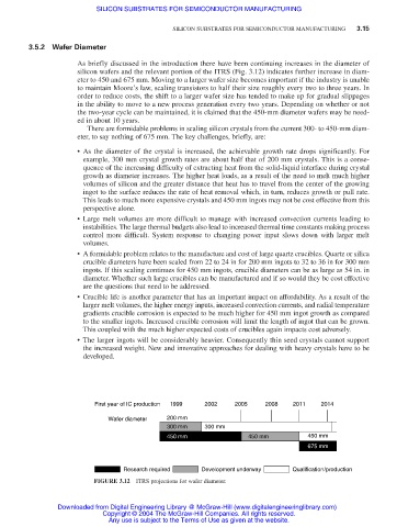
As briefly discussed in the introduction there have been continuing increases in the diameter of
silicon wafers and the relevant portion of the ITRS (Fig. 3.12) indicates further increase in diam-
eter to 450 and 675 mm. Moving to a larger wafer size becomes important if the industry is unable
to maintain Moore’s law, scaling transistors to half their size roughly every two to three years. In
order to reduce costs, the shift to a larger wafer size has tended to make up for gradual slippages
in the ability to move to a new process generation every two years. Depending on whether or not
the two-year cycle can be maintained, it is claimed that the 450-mm diameter wafers may be need-
ed in about 10 years.
There are formidable problems in scaling silicon crystals from the current 300- to 450-mm diam-
eter, to say nothing of 675 mm. The key challenges, briefly, are:
• As the diameter of the crystal is increased, the achievable growth rate drops significantly. For
example, 300 mm crystal growth rates are about half that of 200 mm crystals. This is a conse-
quence of the increasing difficulty of extracting heat from the solid-liquid interface during crystal
growth as diameter increases. The higher heat loads, as a result of the need to melt much higher
volumes of silicon and the greater distance that heat has to travel from the center of the growing
ingot to the surface reduces the rate of heat removal which, in turn, reduces growth or pull rate.
This leads to much more expensive crystals and 450 mm ingots may not be cost effective from this
perspective alone.
• Large melt volumes are more difficult to manage with increased convection currents leading to
instabilities. The large thermal budgets also lead to increased thermal time constants making process
control more difficult. System response to changing power input slows down with larger melt
volumes.
• A formidable problem relates to the manufacture and cost of large quartz crucibles. Quartz or silica
crucible diameters have been scaled from 22 to 24 in for 200 mm ingots to 32 to 36 in for 300 mm
ingots. If this scaling continues for 450 mm ingots, crucible diameters can be as large as 54 in. in
diameter. Whether such large crucibles can be manufactured and if so would they be cost effective
are the questions that need to be addressed.
• Crucible life is another parameter that has an important impact on affordability. As a result of the
larger melt volumes, the higher energy inputs, increased convection currents, and radial temperature
gradients crucible corrosion is expected to be much higher for 450 mm ingot growth as compared
to the smaller ingots. Increased crucible corrosion will limit the length of ingot that can be grown.
This coupled with the much higher expected costs of crucibles again impacts cost adversely.
• The larger ingots will be considerably heavier. Consequently thin seed crystals cannot support
the increased weight. New and innovative approaches for dealing with heavy crystals have to be
developed.
First year of IC production 1999 2002 2005 2008 2011 2014
Wafer diameter 200 mm
300 mm 300 mm
450 mm 450 mm 450 mm
675 mm
Research required Development underway Qualification/production
FIGURE 3.12 ITRS projections for wafer diameter.
Downloaded from Digital Engineering Library @ McGraw-Hill (www.digitalengineeringlibrary.com)
Copyright © 2004 The McGraw-Hill Companies. All rights reserved.
Any use is subject to the Terms of Use as given at the website.