
Page 32 - Semiconductor Manufacturing Handbook
P. 32
Geng(SMH)_CH03.qxd 04/04/2005 19:34 Page 3.11
SILICON SUBSTRATES FOR SEMICONDUCTOR MANUFACTURING
SILICON SUBSTRATES FOR SEMICONDUCTOR MANUFACTURING 3.11
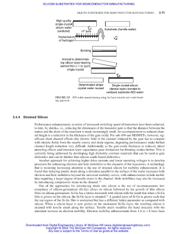
High-quality
single crystal
silicon wafer Substrate (handle wafer)
+
(oxidized) H ions
Implantation
of hydrogen
Bonding
Anneal to delaminate
top silicon layer leaving
behind thin (~1 to 2µm)
single crystal
Delaminated single Single crystal silicon
crystal wafer reused (device layer) bonded to
oxidized substrate-SOI wafer
FIGURE 3.9 SOI wafer manufacturing using the layer transfer and wafer bond-
ing approach.
3.4.4 Strained Silicon
Performance enhancements, in terms of increased switching speed of transistors have been achieved,
to date, by shrinks, i.e., reducing the dimension of the transistor gate so that the distance between the
source and the drain of the transistor is made increasingly small. An accompaniment to reduced chan-
nel length is a reduction in the thickness of the gate oxide. For sub-100-nm MOSFETs, however, sig-
nificant short channel effects (the electric field in the channel induced by the gate has to compete
with electric fields from the nearby source and drain regions, degrading performance) make further
channel length reduction very difficult. Additionally as the gate-oxide thickness is reduced, direct
tunneling effects and inversion layer capacitance pose limitations for thinning oxides further. This is
currently being addressed by developing high dielectric constant materials that can be used as gate
dielectrics and can be thicker than silicon-oxide-based dielectrics.
Another approach for achieving higher drive currents and lower operating voltages is to develop
processes for enhancing electron and hole mobilities in the channels of the transistors. A technology
that is receiving increasing attention is the use of strained silicon for mobility enhancement. It is
found that inducing tensile strain along a direction parallel to the surface of the wafer increases both
electron and hole mobilities beyond the universal mobility curves, with enhancements in hole mobil-
ities requiring a larger degree of tensile strain in the channel. Hole mobilities may also be increased
by introducing compressive strain in the channel. 10
One of the approaches for introducing strain into silicon is the use of incommensurate het-
eroepitaxy of silicon-germanium (Si-Ge) alloys on silicon followed by the growth of thin silicon
films on silicon-germanium. Si-Ge has a lattice mismatch with silicon with the result that when a Si-Ge
11
film is grown on the silicon, the Si-Ge layer is strained. A graded layer of Si-Ge is grown such that
the top region of the Si-Ge film is unstrained but has a different lattice parameter as compared with
silicon. When a silicon layer is now grown on the unstrained Si-Ge layer, the resulting silicon is
strained with tensile strain along the surface. Tensile strain modifies the band structure with the
attendant increase in electron mobility. Electron mobility enhancements from 1.6 to 1.8 have been
Downloaded from Digital Engineering Library @ McGraw-Hill (www.digitalengineeringlibrary.com)
Copyright © 2004 The McGraw-Hill Companies. All rights reserved.
Any use is subject to the Terms of Use as given at the website.