
Page 29 - Semiconductor Manufacturing Handbook
P. 29
Geng(SMH)_CH03.qxd 04/04/2005 19:34 Page 3.8
SILICON SUBSTRATES FOR SEMICONDUCTOR MANUFACTURING
3.8 SEMICONDUCTOR FUNDAMENTALS AND BASIC MATERIALS
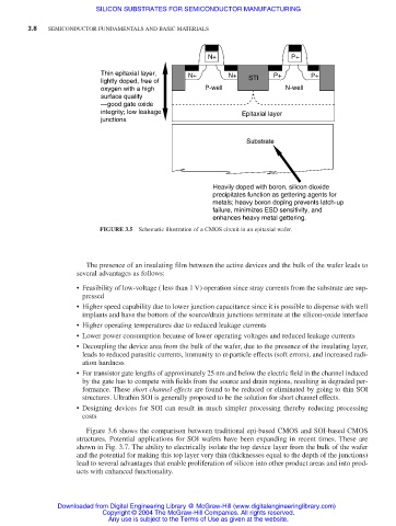
N+ P+
Thin epitaxial layer, N+ N+ P+ P+
lightly doped, free of STI
oxygen with a high P-well N-well
surface quality
—good gate oxide
integrity; low leakage Epitaxial layer
junctions
Substrate
Heavily doped with boron, silicon dioxide
precipitates function as gettering agents for
metals; heavy boron doping prevents latch-up
failure, minimizes ESD sensitivity, and
enhances heavy metal gettering.
FIGURE 3.5 Schematic illustration of a CMOS circuit in an epitaxial wafer.
The presence of an insulating film between the active devices and the bulk of the wafer leads to
several advantages as follows:
• Feasibility of low-voltage ( less than 1 V) operation since stray currents from the substrate are sup-
pressed
• Higher speed capability due to lower junction capacitance since it is possible to dispense with well
implants and have the bottom of the source/drain junctions terminate at the silicon-oxide interface
• Higher operating temperatures due to reduced leakage currents
• Lower power consumption because of lower operating voltages and reduced leakage currents
• Decoupling the device area from the bulk of the wafer, due to the presence of the insulating layer,
leads to reduced parasitic currents, immunity to a-particle effects (soft errors), and increased radi-
ation hardness
• For transistor gate lengths of approximately 25 nm and below the electric field in the channel induced
by the gate has to compete with fields from the source and drain regions, resulting in degraded per-
formance. These short channel effects are found to be reduced or eliminated by going to thin SOI
structures. Ultrathin SOI is generally proposed to be the solution for short channel effects.
• Designing devices for SOI can result in much simpler processing thereby reducing processing
costs
Figure 3.6 shows the comparison between traditional epi-based CMOS and SOI-based CMOS
structures. Potential applications for SOI wafers have been expanding in recent times. These are
shown in Fig. 3.7. The ability to electrically isolate the top device layer from the bulk of the wafer
and the potential for making this top layer very thin (thicknesses equal to the depth of the junctions)
lead to several advantages that enable proliferation of silicon into other product areas and into prod-
ucts with enhanced functionality.
Downloaded from Digital Engineering Library @ McGraw-Hill (www.digitalengineeringlibrary.com)
Copyright © 2004 The McGraw-Hill Companies. All rights reserved.
Any use is subject to the Terms of Use as given at the website.