
Page 26 - Semiconductor Manufacturing Handbook
P. 26
Geng(SMH)_CH03.qxd 04/04/2005 19:34 Page 3.5
SILICON SUBSTRATES FOR SEMICONDUCTOR MANUFACTURING
SILICON SUBSTRATES FOR SEMICONDUCTOR MANUFACTURING 3.5
3.4.1 Silicon as an Active Substrate Material
A large class of devices is manufactured using polished silicon wafers as substrate materials. These
include many discrete devices such as transistors, power and RF devices, and, very importantly, dynam-
ic random access memories (DRAMs). As is well known, silicon wafers can be controllably doped dur-
ing crystal growth and the wafers in turn can be selectively doped using gas phase diffusion or ion
implantation processes for the manufacture of a large complement of complex devices and circuits.
Polished silicon wafers represent the lowest cost version of this material for both discrete-device
and integrated circuit manufacture. A key aspect of polished silicon wafers for the manufacture of
advanced integrated circuits is the need for a preprocess step, prior to device fabrication, which mod-
ifies the surface and near surface characteristics of the wafer. Since silicon crystal growth is done by
melting silicon in a quartz crucible, a necessary accompaniment to this process is the dissolution of
the quartz in the molten silicon and the attendant incorporation of oxygen in the crystal. The subse-
quently sliced and polished wafers will have a distribution of oxygen throughout the bulk as well as
at the surface. The key effects of oxygen are as follows:
• Interstitial oxygen is a donor in silicon, altering the electrical characteristics of the material.
Annealing the ingots can cause the oxygen to move from the interstitial, electrically active, loca-
tions in the crystal, thus eliminating the electrical effects. A donor anneal process is a frequent step
following the production of the ingot.
• Oxygen at the surface of the wafer can introduce adverse effects in shallow p-n junctions and at
the silicon-silicon dioxide interface, causing excessive leakage, premature breakdown, a compro-
mise in the integrity of gate oxides, and a variation of the electrical parameters across the wafer.
• Oxygen, when converted into oxide precipitates (silicon dioxide) can function as internal gettering
agents to attract and trap fast-diffusing heavy metals in wafers. However, this has to be achieved
in such a way that oxide precipitates are not present at the surface as their presence would have
severe negative electrical consequences in devices.
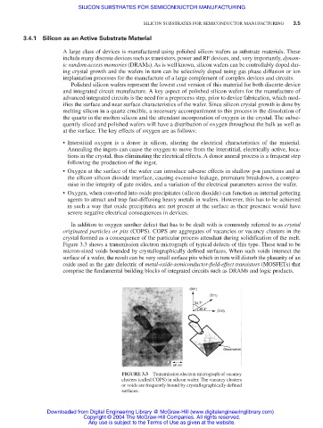
In addition to oxygen another defect that has to be dealt with is commonly referred to as crystal
originated particles or pits (COPS). COPS are aggregates of vacancies or vacancy clusters in the
crystal formed as a consequence of the particular process attendant during solidification of the melt.
Figure 3.3 shows a transmission electron micrograph of typical defects of this type. These tend to be
micron-sized voids bounded by crystallographically defined surfaces. When such voids intersect the
surface of a wafer, the result can be very small surface pits which in turn will disturb the planarity of an
oxide used as the gate dielectric of metal-oxide-semiconductor-field-effect transistors (MOSFETs) that
comprise the fundamental building blocks of integrated circuits such as DRAMs and logic products.
(001)
(111)
54.7°
35.3°
(110)
Observation
50 nm
FIGURE 3.3 Transmission electron micrograph of vacancy
clusters (called COPS) in silicon wafer. The vacancy clusters
or voids are frequently bound by crystallographically defined
surfaces.
Downloaded from Digital Engineering Library @ McGraw-Hill (www.digitalengineeringlibrary.com)
Copyright © 2004 The McGraw-Hill Companies. All rights reserved.
Any use is subject to the Terms of Use as given at the website.