
Page 25 - Semiconductor Manufacturing Handbook
P. 25
Geng(SMH)_CH03.qxd 04/04/2005 19:34 Page 3.4
SILICON SUBSTRATES FOR SEMICONDUCTOR MANUFACTURING
3.4 SEMICONDUCTOR FUNDAMENTALS AND BASIC MATERIALS
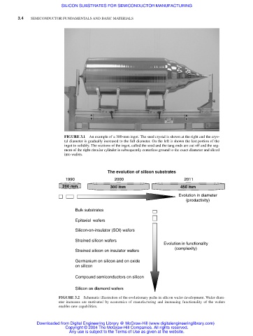
FIGURE 3.1 An example of a 300-mm ingot. The seed crystal is shown at the right and the crys-
tal diameter is gradually increased to the full diameter. On the left is shown the last portion of the
ingot to solidify. The sections of the ingot, called the seed and the tang ends are cut off and the seg-
ment of the right circular cylinder is subsequently centerless ground to the exact diameter and sliced
into wafers.
The evolution of silicon substrates
1990 2000 2011
200 mm 300 mm 450 mm
Evolution in diameter
(productivity)
Bulk substrates
Epitaxial wafers
Silicon-on-insulator (SOI) wafers
Strained silicon wafers
Evolution in functionality
(complexity)
Strained silicon on insulator wafers
Germanium on silicon and on oxide
on silicon
Compound semiconductors on silicon
Silicon on diamond wafers
FIGURE 3.2 Schematic illustration of the evolutionary paths in silicon wafer development. Wafer diam-
eter increases are motivated by economics of manufacturing and increasing functionality of the wafers
enables new capabilities.
Downloaded from Digital Engineering Library @ McGraw-Hill (www.digitalengineeringlibrary.com)
Copyright © 2004 The McGraw-Hill Companies. All rights reserved.
Any use is subject to the Terms of Use as given at the website.