
Page 15 - Semiconductor Manufacturing Handbook
P. 15
Geng(SMH)_CH02.qxd 04/04/2005 19:33 Page 2.2
IC DESIGN
2.2 SEMICONDUCTOR FUNDAMENTALS AND BASIC MATERIALS
designs. An FPGA is a reprogrammable logic device that uses gate arrays to implement the user’s
design.
A very common type of ASIC is a digital signal processor (DSP). This is a microprocessor that
is usually designed to measure or manipulate a continuous real-world analog signal in a digital
domain. The analog signal coming into the DSP is converted into a digital representation by the DSP.
When leaving the IC, the digital signal can pass through a digital-to-analog converter and be output
as an analog signal.
2.3 THE P-N JUNCTION
Silicon itself is a semiconductive element and is not suitable for conducting current on its own.
However, when impurities such as gallium, boron, or aluminum are added, thereby doping the
silicon, a deficiency of electrons is created in the silicon, giving it a positive bias. The absence of an
electron in the silicon molecule is commonly called a “hole.” This type of doped silicon is commonly
referred to as p-type.
Similarly, if silicon is doped with an impurity such as arsenic or antimony, then an excess of free
electrons is created, thus creating a negative bias. This type of doped silicon is known as n-type.
When p- and n-type silicon are placed in contact with each other, the junction of these two mate-
rials allows electric current to flow in one direction from p to n, but not in the other. This p-n junction
is the basic building block of many types of electronic devices such as the diode and the transistor.
2.4 THE TRANSISTOR
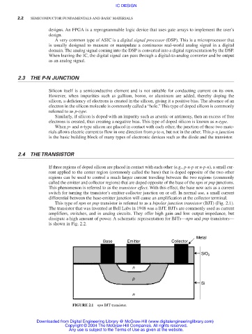
If three regions of doped silicon are placed in contact with each other (e.g., p-n-p or n-p-n), a small cur-
rent applied to the center region (commonly called the base) that is doped opposite of the two other
regions can be used to control a much larger current traveling between the two regions (commonly
called the emitter and collector regions) that are doped opposite of the base of the npn or pnp junctions.
This phenomenon is referred to as the transistor effect. With this effect, the base now acts as a current
switch for turning the transistor’s emitter-collector junction on or off. In normal use, a small current
differential between the base-emitter junction will cause an amplification at the collector terminal.
This type of npn or pnp transistor is referred to as a bipolar junction transistor (BJT) (Fig. 2.1).
The transistor that was invented at Bell Labs in 1948 was a BJT. BJTs are commonly used as current
amplifiers, switches, and in analog circuits. They offer high gain and low output impedance, but
dissipate a high amount of power. A schematic representation for BJTs—npn and pnp transistors—
is shown in Fig. 2.2.
Metal
Base Emitter Collector
SiO 2
n
p
Si
n
FIGURE 2.1 npn BJT transistor.
Downloaded from Digital Engineering Library @ McGraw-Hill (www.digitalengineeringlibrary.com)
Copyright © 2004 The McGraw-Hill Companies. All rights reserved.
Any use is subject to the Terms of Use as given at the website.