
Page 10 - Semiconductor Manufacturing Handbook
P. 10
Geng(SMH)_CH01.qxd 04/04/2005 19:32 Page 1.9
HOW SEMICONDUCTOR CHIPS ARE MADE
HOW SEMICONDUCTOR CHIPS ARE MADE 1.9
process steps of how to transfer a pattern onto the silicon wafer. The sequence of the process steps
patterns exactly one layer of the semiconductor material, and the same sequence patterns the layer
of the complete surface of the wafer. Thus, hundreds of millions of patterns are transferred to semi-
conductor surface simultaneously.
1.6.5 Layering
To introduce a polygon layer, a second and thinner layer of silicon dioxide is grown from thermal
oxidation as before over the ridges and etched areas of the wafer base (Fig. 1.4(a)). Then a layer of
polysilicon (Fig. 1.4(b)) and another layer of the photoresist (Fig. 1.4(c)) are evenly spread on the
wafer.
The photolithography process is applied to define the polygon region. Ultraviolet light exposes the
photoresist through a second mask, leaving a new pattern for polysilicon on the photoresist (Fig. 1.4(d)).
The photoresist is dissolved with a solvent to expose the polysilicon and silicon dioxide, which are then
etched away with chemicals (Fig. 1.4(e)). After the remaining photoresist is removed (Fig. 1.4( f )),
ridges of polysilicon and silicon dioxide are left on the polygon region. Figure 1.4 illustrates the process
steps of how to transfer another polysilicon layer on the previous layer.
A similar process will be repeated over and over again with each mask to pattern different layers of
deposited materials. During this manufacturing process, conductive regions are formed and insulated
from each other. Later they are selectively connected to each other to produce an integrated circuit.
1.6.6 Doping: Diffusion and Ion Implantation
Many steps in the IC manufacturing process require a change in the dopant concentration of some
areas to make them more conductive. Two approaches are used to introduce dopants—diffusion and
ion implantation.
Diffusion implantation is performed by either exposing the wafer to a high-temperature environ-
ment of dopant vapor (gaseous diffusion) or predepositing dopant ions on the surface and then ther-
mally driving them in by high-temperature processing (nongaseous diffusion). The final
concentration is greatest at the surface and decreases deeper in the material.
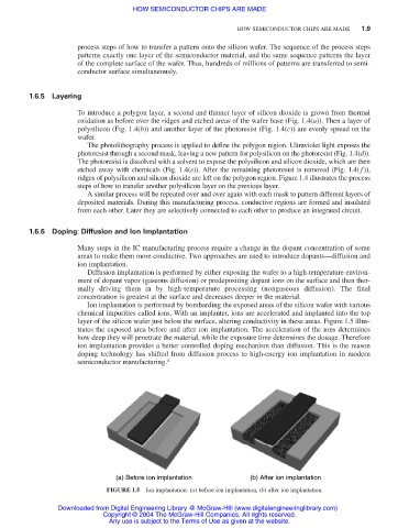
Ion implantation is performed by bombarding the exposed areas of the silicon wafer with various
chemical impurities called ions. With an implanter, ions are accelerated and implanted into the top
layer of the silicon wafer just below the surface, altering conductivity in these areas. Figure 1.5 illus-
trates the exposed area before and after ion implantation. The acceleration of the ions determines
how deep they will penetrate the material, while the exposure time determines the dosage. Therefore
ion implantation provides a better controlled doping mechanism than diffusion. This is the reason
doping technology has shifted from diffusion process to high-energy ion implantation in modern
semiconductor manufacturing. 4
(a) Before ion implantation (b) After ion implantation
FIGURE 1.5 Ion implantation: (a) before ion implantation, (b) after ion implantation.
Downloaded from Digital Engineering Library @ McGraw-Hill (www.digitalengineeringlibrary.com)
Copyright © 2004 The McGraw-Hill Companies. All rights reserved.
Any use is subject to the Terms of Use as given at the website.