
Page 7 - Semiconductor Manufacturing Handbook
P. 7
Geng(SMH)_CH01.qxd 04/04/2005 19:32 Page 1.6
HOW SEMICONDUCTOR CHIPS ARE MADE
1.6 SEMICONDUCTOR FUNDAMENTALS AND BASIC MATERIALS
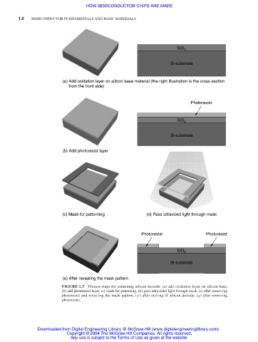
SiO 2
Si-substrate
(a) Add oxidation layer on silicon base material (the right illustration is the cross section
from the front side)
Photoresist
SiO 2
Si-substrate
(b) Add photoresist layer
(c) Mask for patterning (d) Pass ultraviolet light through mask
Photoresist Photoresist
SiO 2
Si-substrate
(e) After revealing the mask pattern
FIGURE 1.3 Process steps for patterning silicon dioxide: (a) add oxidation layer on silicon base,
(b) add photoresist layer, (c) mask for patterning, (d) pass ultraviolet light through mask, (e) after removing
photoresist and revealing the mask pattern, ( f ) after etching of silicon dioxide, (g) after removing
photoresist.
Downloaded from Digital Engineering Library @ McGraw-Hill (www.digitalengineeringlibrary.com)
Copyright © 2004 The McGraw-Hill Companies. All rights reserved.
Any use is subject to the Terms of Use as given at the website.