
Page 9 - Semiconductor Manufacturing Handbook
P. 9
Geng(SMH)_CH01.qxd 04/04/2005 19:32 Page 1.8
HOW SEMICONDUCTOR CHIPS ARE MADE
1.8 SEMICONDUCTOR FUNDAMENTALS AND BASIC MATERIALS
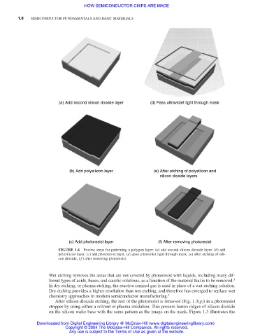
(a) Add second silicon dioxide layer (d) Pass ultraviolet light through mask
(b) Add polysilicon layer (e) After etching of polysilicon and
silicon dioxide layers
(c) Add photoresist layer (f) After removing photoresist
FIGURE 1.4 Process steps for patterning a polygon layer: (a) add second silicon dioxide layer, (b) add
polysilicon layer, (c) add photoresist layer, (d) pass ultraviolet light through mask, (e) after etching of sili-
con dioxide, ( f ) after removing photoresist.
Wet etching removes the areas that are not covered by photoresist with liquids, including many dif-
ferent types of acids, bases, and caustic solutions, as a function of the material that is to be removed. 3
In dry etching, or plasma etching, the reactive ionized gas is used in place of a wet-etching solution.
Dry etching provides a higher resolution than wet etching, and therefore has emerged to replace wet
chemistry approaches in modern semiconductor manufacturing. 4
After silicon dioxide etching, the rest of the photoresist is removed (Fig. 1.3(g)) in a photoresist
stripper by using either a solvent or plasma oxidation. This process leaves ridges of silicon dioxide
on the silicon wafer base with the same pattern as the image on the mask. Figure 1.3 illustrates the
Downloaded from Digital Engineering Library @ McGraw-Hill (www.digitalengineeringlibrary.com)
Copyright © 2004 The McGraw-Hill Companies. All rights reserved.
Any use is subject to the Terms of Use as given at the website.