
Page 11 - Semiconductor Manufacturing Handbook
P. 11
Geng(SMH)_CH01.qxd 04/04/2005 19:32 Page 1.10
HOW SEMICONDUCTOR CHIPS ARE MADE
1.10 SEMICONDUCTOR FUNDAMENTALS AND BASIC MATERIALS
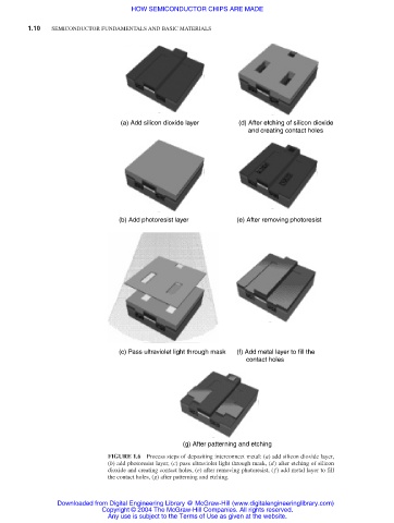
(a) Add silicon dioxide layer (d) After etching of silicon dioxide
and creating contact holes
(b) Add photoresist layer (e) After removing photoresist
(c) Pass ultraviolet light through mask (f) Add metal layer to fill the
contact holes
(g) After patterning and etching
FIGURE 1.6 Process steps of depositing interconnect metal: (a) add silicon dioxide layer,
(b) add photoresist layer, (c) pass ultraviolet light through mask, (d) after etching of silicon
dioxide and creating contact holes, (e) after removing photoresist, ( f) add metal layer to fill
the contact holes, (g) after patterning and etching.
Downloaded from Digital Engineering Library @ McGraw-Hill (www.digitalengineeringlibrary.com)
Copyright © 2004 The McGraw-Hill Companies. All rights reserved.
Any use is subject to the Terms of Use as given at the website.