Page 17 - Semiconductor Manufacturing Handbook
P. 17

Geng(SMH)_CH02.qxd  04/04/2005  19:33  Page 2.4


                                                         IC DESIGN

                   2.4  SEMICONDUCTOR FUNDAMENTALS AND BASIC MATERIALS

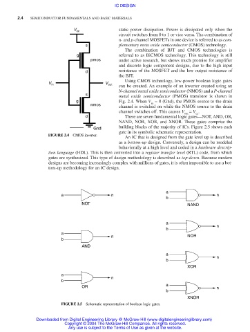
                                         V cc              static power dissipation. Power is dissipated only when the
                                                           circuit switches from 0 to 1 or vice versa. The combination of
                                                           n- and p-channel MOSFETs in one device is referred to as com-
                                              s            plementary meta oxide semiconductor (CMOS) technology.
                                                             The combination of BJT and CMOS technologies is
                                          g                referred to as BiCMOS technology. This technology is still
                                                pmos       under active research, but shows much promise for amplifier
                                                           and discrete logic component designs, due to the high input
                                             d             resistance of the MOSFET and the low output resistance of
                                                           the BJT.
                                                             Using CMOS technology, low-power boolean logic gates
                               V in                  V out  can be created. An example of an inverter created using an
                                                           N-channel metal oxide semiconductor (NMOS) and a P-channel
                                              s
                                                           metal oxide semiconductor  (PMOS) transistor is shown in
                                          g                Fig. 2.4. When V = 0 (Gnd), the PMOS source to the drain
                                                                       in
                                                nmos       channel is switched on while the NMOS source to the drain
                                                           channel switches off. This causes V  = V .
                                                                                    out   cc
                                             d               There are seven fundamental logic gates—NOT, AND, OR,
                                                           NAND, NOR, XOR, and XNOR.  These gates comprise the
                                                 Gnd       building blocks of the majority of ICs. Figure 2.5 shows each
                                                           gate in its symbolic schematic representation.
                               FIGURE 2.4  CMOS inverter.
                                                             An IC that is designed from the gate level up is described
                                                           as a bottom-up design. Conversely, a design can be modeled
                                                           behaviorally at a high level and coded in a hardware descrip-
                               tion language (HDL). This is then converted into a register transfer level (RTL) code, from which
                               gates are synthesized. This type of design methodology is described as top-down. Because modern
                               designs are becoming increasingly complex with millions of gates, it is often impossible to use a bot-
                               tom-up methodology for an IC design.


                                                                             a
                                    a                   n                                        n
                                                                             b
                                            NOT                                      NAND


                                                                             a
                                                                                                 n
                                                                             b
                                    a
                                                        n                            NOR
                                    b
                                            AND
                                                                             a
                                                                                                 n
                                                                             b
                                                                                     XOR
                                    a
                                                        n
                                    b
                                                                             a
                                            OR                                                   n
                                                                             b
                                                                                     XNOR
                                    FIGURE 2.5  Schematic representation of boolean logic gates.


                          Downloaded from Digital Engineering Library @ McGraw-Hill (www.digitalengineeringlibrary.com)
                                     Copyright © 2004 The McGraw-Hill Companies. All rights reserved.
                                       Any use is subject to the Terms of Use as given at the website.
   12   13   14   15   16   17   18   19   20   21   22