
Page 152 - Six Sigma for electronics design and manufacturing
P. 152
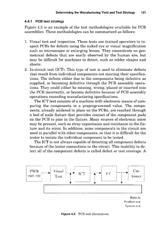
4.4.1 PCB test strategy
                        Figure 4.5 is an example of the test methodologies available for PCB
                        assemblies. These methodologies can be summarized as follows:
                        1. Visual test and inspection. These tests use trained operators to in-
                          spect PCBs for defects using the naked eye or visual magnification
                          such as microscopes or enlarging lenses. They concentrate on geo-
                          metrical  defects  that  are  easily  observed  by  the  human  eye,  but
                          may be difficult for machines to detect, such as solder shapes and
                          shorts.      Determining the Manufacturing Yield and Test Strategy  121
                        2. In-circuit test (ICT). This type of test is used to eliminate defects
                          that result from individual components not meeting their specifica-
                          tions. The defects either due to the components being defective as
                          supplied, or becoming defective through the PCB assembly opera-
                          tions. They could either be missing, wrong, placed or inserted into
                          the PCB incorrectly, or become defective because of PCB assembly
                          operations exceeding manufacturing specifications.
                            The ICT test consists of a machine with electronic means of com-
                          paring  the  components  to  a  preprogrammed  value.  The  compo-
                          nents, already soldered in place on the PCBs, are reached through
                          a bed of nails fixture that provides contact of the component pads
                          on the PCB to pins in the fixture. Many sources of electronic noise
                          may be present, such as stray capacitance and resistance in the fix-
                          ture and its wires. In addition, some components in the circuit are
                          used in parallel with other components, so that it is difficult for the
                          tester to isolate the individual component to be tested.
                            The ICT is not always capable of detecting all component defects
                          because of the tester connections to the circuit. This inability to de-
                          tect all of the component defects is called defect or test coverage. A


                                         Figure 4.5 PCB test alternatives.