
Page 156 - Six Sigma for electronics design and manufacturing
P. 156
Determining the Manufacturing Yield and Test Strategy
PCBs. Therefore, most companies would opt for the non-visual test
strategy, because automatic testing is usually more predictable than
manual inspection. In addition, in-circuit testing can be improved
with better equipment, whereas visual testing would not greatly in-
crease in efficiency with increased operator experience.
In order to properly devise the best strategy for scenario 1, more in-
formation will have to be collected. This would include the capital and
depreciation costs of the in-circuit equipment and fixtures, as well as
the resources needed to maintain and repair them. More discussion is
given on that in Chapter 6. 125
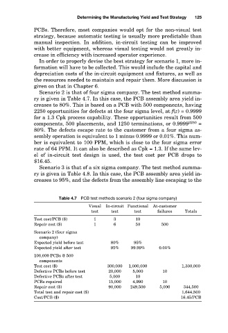
Scenario 2 is that of four sigma company. The test method summa-
ry is given in Table 4.7. In this case, the PCB assembly area yield in-
creases to 80%. This is based on a PCB with 500 components, having
2250 opportunities for defects at the four sigma level, at f(z) = 0.9999
for a 1.3 Cpk process capability. These opportunities result from 500
components, 500 placements, and 1250 terminations, or 0.9999 2250 =
80%. The defects escape rate to the customer from a four sigma as-
sembly operation is equivalent to 1 minus 0.9999 or 0.01%. This num-
ber is equivalent to 100 PPM, which is close to the four sigma error
rate of 64 PPM. It can also be described as Cpk = 1.3. If the same lev-
el of in-circuit test design is used, the test cost per PCB drops to
$16.45.
Scenario 3 is that of a six sigma company. The test method summa-
ry is given in Table 4.8. In this case, the PCB assembly area yield in-
creases to 95%, and the defects from the assembly line escaping to the
Table 4.7 PCB test methods scenario 2 (four sigma company)
Visual In-circuit Functional At-customer
test test test failures Totals
Test cost/PCB ($) 1 3 10
Repair cost ($) 1 6 50 500
Scenario 2 (four sigma
company)
Expected yield before test 80% 95%
Expected yield after test 95% 99.99% 0.01%
100,000 PCBs @ 500
components
Test cost ($) 300,000 1,000,000 1,300,000
Defective PCBs before test 20,000 5,000 10
Defective PCBs after test 5,000 10
PCBs repaired 15,000 4,990 10
Repair cost ($) 90,000 249,500 5,000 344,500
Total test and repair cost ($) 1,644,500
Cost/PCB ($) 16.45/PCB