
Page 87 - Six Sigma for electronics design and manufacturing
P. 87
Six Sigma for Electronics Design and Manufacturing
56
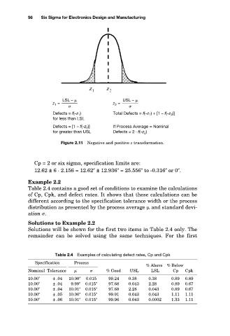
LSL – USL –
z 1 = z 2 =
Defects = f(–z 1 ) Total Defects = f(–z 1 ) + [1 – f(–z 2 )]
for less than LSL
Defects = [1 – f(–z 2 )] If Process Average = Nominal
for greater than USL Defects = 2 · f(–z 2 )
Figure 2.11 Negative and positive z transformation.
Cp = 2 or six sigma, specification limits are:
12.62 ± 6 · 2.156 = 12.62 ± 12.936 = 25.556 to -0.316 or 0 .
Example 2.2
Table 2.4 contains a good set of conditions to examine the calculations
of Cp, Cpk, and defect rates. It shows that these calculations can be
different according to the specification tolerance width or the process
distribution as presented by the process average and standard devi-
ation .
Solutions to Example 2.2
Solutions will be shown for the first two items in Table 2.4 only. The
remainder can be solved using the same techniques. For the first
Table 2.4 Examples of calculating defect rates, Cp and Cpk
Specification Process
___________________ ______________ % Above % Below
Nominal Tolerance % Good USL LSL Cp Cpk
10.00 ± .04 10.00 0.015 99.24 0.38 0.38 0.89 0.89
10.00 ± .04 9.99 0.015 97.68 0.043 2.28 0.89 0.67
10.00 ± .04 10.01 0.015 97.68 2.28 0.043 0.89 0.67
10.00 ± .05 10.00 0.015 99.91 0.043 0.043 1.11 1.11
10.00 ± .06 10.01 0.015 99.96 0.043 0.0002 1.33 1.11