
Page 99 - The Art and Science of Analog Circuit Design
P. 99
Signal Conditioning in Oscilloscopes and the Spirit of Invention
the input drives the gate, source, and drain of the FET through an equal
change via the 20pF input capacitor and the gate-drain and gate-source
capacitances. Since all three terminals of the FET remain at the same
voltage, the FET is safe from overvoltage stress. Of course, the switches
must have very low capacitance in the open state, or capacitive voltage
division would allow the terminals of the FET to see differing voltages.
In ~ 100 mode, the floating FET will see 40V excursions (eight divisions
on the oscilloscope screen at 5V per division) as a matter of course. For
this reason the -1 protection diodes must be switched to a higher bias
voltage (±50V) when in the -r 10 and ^-100 modes. The switches that con-
trol the voltage on the protection diodes are not involved in the high-
frequency performance of the front-end and therefore can be
implemented with slow, high-voltage semiconductors.
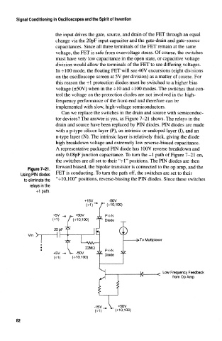
Can we replace the switches in the drain and source with semiconduc-
tor devices? The answer is yes, as Figure 7-21 shows. The relays in the
drain and source have been replaced by PIN diodes. PIN diodes are made
with a p-type silicon layer (P), an intrinsic or undoped layer (I), and an
n-type layer (N). The intrinsic layer is relatively thick, giving the diode
high breakdown voltage and extremely low reverse-biased capacitance.
A representative packaged PIN diode has 100V reverse breakdown and
only O.OSpF junction capacitance. To turn the -f-1 path of Figure 7-21 on,
the switches are all set to their "-fl" positions. The PIN diodes are then
forward biased, the bipolar transistor is connected to the op amp, and the
Figure 7-21.
Using PIN diodes FET is conducting. To turn the path off, the switches are set to their
to eliminate the "-r 10,100" positions, reverse-biasing the PIN diodes. Since these switches
relays in the
~1 path.
-50V
(•M0.100)
+5V _ fr- +50V
(-5-1) / (-5-10,100)
20 pF
Vin
To Multiplexor
V -50V
(-=-10,100)
Low Frequency Feedback
from Op Amp
+50V
(-M0.100)
82