
Page 95 - The Art and Science of Analog Circuit Design
P. 95
Signal Conditioning in Oscilloscopes and the Spirit of Invention
nearly constant, independent of the switch positions. This requirement
assures that we maintain attenuation accuracy and flatness for all four
combinations of attenuator relay settings.
Dividing by a high ratio such as 125 is similar to trying to build a high-
isolation switch; the signal attempts to bypass the divider, causing feed-
through problems. If we set a standard for feedthrough of less than one
least-significant bit in an 8-bit digital oscilloscope, the attenuator must
s
isolate the input from the output by 201og 10(125 -2 ) = 90dB! I once spent
two months tracking down such an isolation problem and traced it to
wave guide propagation and cavity resonance at 2GHz inside the metallic
attenuator cover.
Relays are used for the switches because they have low contact im-
pedance, high isolation, and high withstanding voltages. However, in a
realm where 1mm of wire looks like a transmission line, the relays have
dreadful parasitics. To make matters worse, the relays are large enough
to spread the attenuator out over an area of about 2 x 3cm, Assuming a
propagation velocity of half the speed of light, three centimeters takes
200ps, which is dangerously close to the 700ps rise time of a 500MHz
oscilloscope. In spite of the fact that I have said we can have no trans-
mission lines in a high-impedance attenuator, we have to deal with them
anyway! To deal with transmission line and parasitic reactance effects, a
real attenuator includes many termination and damping resistors not
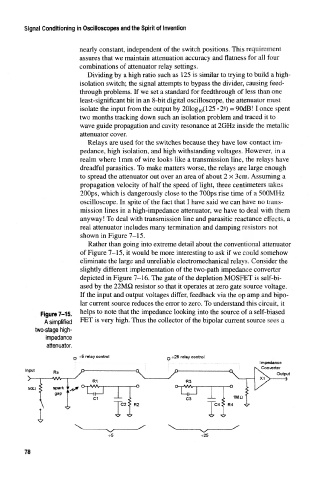
shown in Figure 7-15.
Rather than going into extreme detail about the conventional attenuator
of Figure 7-15, it would be more interesting to ask if we could somehow
eliminate the large and unreliable electromechanical relays. Consider the
slightly different implementation of the two-path impedance converter
depicted in Figure 7-16. The gate of the depletion MOSFET is self-bi-
ased by the 22MO resistor so that it operates at zero gate source voltage.
If the input and output voltages differ, feedback via the op amp and bipo-
lar current source reduces the error to zero. To understand this circuit, it
helps to note that the impedance looking into the source of a self-biased
Figure 7-15.
A simplified FET is very high. Thus the collector of the bipolar current source sees a
two-stage high-
impedance
attenuator,
-=-5 relay control j-25 relay control
Impedance
Converter
Input
Output
X1 "
78