
Page 92 - The Art and Science of Analog Circuit Design
P. 92
Steve Roach
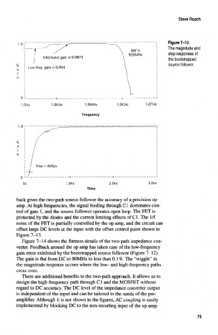
i.o Figure 7-12.
The magnitude and
BWis
920MHz step responses of
Mid-band gain is 0.9875
the bootstrapped
source follower.
Low freq. gain is 0.904
0 j _ . j . .
I.OHz 1.0KHz 1.0MHz 1 .OTHz
Frequency
Trise = 400ps
i_ i
Os 1.0ns 2.0ns 3.0ns
Time
back gives the two-path source follower the accuracy of a precision op
amp. At high frequencies, the signal feeding through Cl dominates con-
trol of gate 1, and the source follower operates open loop. The FET is
protected by the diodes and the current limiting effects of Cl. The 1/f
noise of the FET is partially controlled by the op amp, and the circuit can
offset large DC levels at the input with the offset control point shown in
Figure 7-13.
Figure 7-14 shows the flatness details of the two-path impedance con-
verter. Feedback around the op amp has taken care of the low-frequency
gain error exhibited by the bootstrapped source follower (Figure 7-12).
The gain is flat from DC to 80MHz to less than 0.1%. The "wiggle" in
the magnitude response occurs where the low- and high-frequency paths
cross over.
There are additional benefits to the two-path approach. It allows us to
design the high-frequency path through Cl and the MOSFET without
regard to DC accuracy. The DC level of the impedance converter output
is independent of the input and can be tailored to the needs of the pre-
amplifier. Although it is not shown in the figures, AC coupling is easily
implemented by blocking DC to the non-inverting input of the op amp.
75