
Page 88 - The Art and Science of Analog Circuit Design
P. 88
Steve Roach
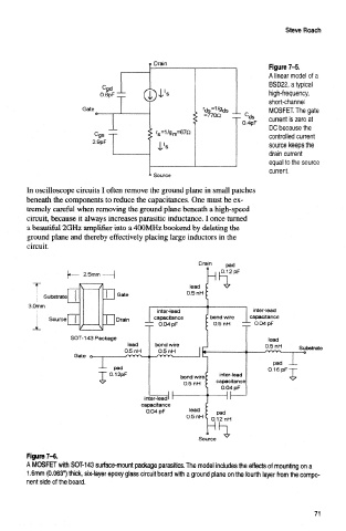
P Drain
Figure 7-5.
A linear model of a
BSD22, a typical
c
gd
high-frequency,
short-channel
Gate r ds =1/ 9ds MOSFET. The gate
T =770Q 0.4pF current is zero at
u r s=1/g m=67a DC because the
gs controlled current
2.9pF
source keeps the
drain current
equal to the source
current.
° Source
In oscilloscope circuits I often remove the ground plane in small patches
beneath the components to reduce the capacitances. One must be ex-
tremely careful when removing the ground plane beneath a high-speed
circuit, because it always increases parasitic inductance. I once turned
a beautiful 2GrHz amplifier into a 400MHz bookend by deleting the
ground plane and thereby effectively placing large inductors in the
circuit.
Drain pad
,0.12 pF
lead
\ Substrate Gate 0.5 nH
3.Omm
inter-lead inter-lead
! Source Drain capacitance bond wire capacitance
±1 O.O4 pF 0.5 nH I 0.04 pF
SOT-143 Package
lead bond wire
0.5 nH O.5nH Substrate
Gate o-
T pad
I 0.12pF bond wirej capacitance
inter-lead
0.5 nH
0.04 pF
inter-lead'
capacitance
0.04 pF lead pad
0.5 nH 0.12 nH
Source
Figure 7-6.
A MOSFET with SOT-143 surface-mount package parasitics. The model includes the effects of mounting on a
1.6mm (0.063*) thick, six-layer epoxy glass circuit board with a ground plane on the fourth layer from the compo-
nent side of the board.
71