
Page 91 - The Art and Science of Analog Circuit Design
P. 91
Signal Conditioning in Oscilloscopes and the Spirit of invention
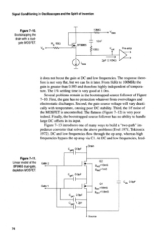
Figure 7-10. 10MQ
'bias
Bootstrapping the
drain with a dual-
1QnF
gate MOSFET.
BF996S
2pF || 10KQ
bias
it does not boost the gain at DC and low frequencies. The response there-
fore is not very flat, but we can fix it later. From 1kHz to 100MHz the
gain is greater than 0.985 and therefore highly independent of tempera-
ture. The 1 % settling time is very good at 1 .Ons.
Several problems remain in the bootstrapped source follower of Figure
7-10. First, the gate has no protection whatever from overvoltages and
electrostatic discharges. Second, the gate-source voltage will vary drasti-
cally with temperature, causing poor DC stability. Third, the 1/f noise of
the MOSFET is uncontrolled. The flatness (Figure 7-12) is very poor
indeed. Finally, the bootstrapped source follower has no ability to handle
large DC offsets in its input.
Figure 7-13 introduces one of many ways to build a "two-path" im-
pedance converter that solves the above problems (Evel 1971, Tektronix
1972). DC and low frequencies flow through the op amp, whereas high
frequencies bypass the op amp via C1. At DC and low frequencies, feed-
Drain
Figure 7-11.
Linear model of the Gate 2
BF996S dual-gate,
depletion MOSFET,
•*ds
Gatel
Source
74