
Page 96 - The Art and Science of Analog Circuit Design
P. 96
Steve Roach
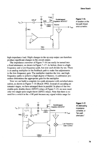
Drain
«20pF f~ Bootstrapped Figure 7-16.
Gate r~| Depletion MOSFET A variation on the
two-path imped-
I—vw,— Source
22MQ ance converter.
-*v out
MMQ
-A/W-
high-impedance load. Slight changes in the op amp output can therefore
produce significant changes in the circuit output.
The impedance converter of Figure 7-16 can easily be turned into
a fixed attenuator, as shown in Figure 7-17. As before, there is a high-
frequency and a low-frequency path, but now each divides by ten. There
is an analog multiplier in the feedback path to make fine adjustments
to the low-frequency gain. The multiplier matches the low- and high-
frequency paths to achieve a high degree of flatness. A calibration pro-
cedure determines the appropriate gain for the multiplier.
Now we can build a complete two-path attenuator with switched atten-
uation, as shown in Figure 7-18 (Roach 1992). Instead of cascading at-
tenuator stages, we have arranged them in parallel. In place of the two
double-pole double-throw (DPDT) relays of Figure 7-15, we now need
only two single-pole single-throw (SPST) relays. Note that there is no
need for a switch in the -rl 00 path because any signal within range for
Figure 7-17.
•MO
Bootstrapped An attenuating
Depletion MOSFET
impedance
converter, or
"two-path
attenuator."
Low frequency
Gain Control
79