
Page 89 - The Art and Science of Analog Circuit Design
P. 89
Signal Conditioning in Oscilloscopes and the Spirit of Invention
1 mm Trace 0.1 pF
1 mm Trace
i
0.6nH R 0.7nH i Q,6nH
rwv\ . i. j _rw>r\.
r I J
I V \rV """""~
I 29fF ! — L pad pad —L I
29fF : ; 29fF
-r 0.1 5pF 0.1 5pF -T- j
I l\
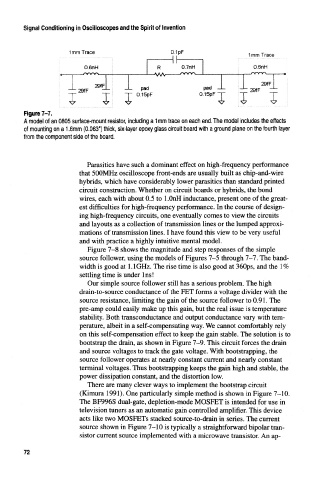
Figure 7-7.
A model of an 0805 surface-mount resistor, including a 1mm trace on each end. The model includes the-effects
of mounting on a 1.6mm (0.063") thick, six-layer epoxy glass circuit board with a ground plane on the fourth layer
from the component side of the board.
Parasitics have such a dominant effect on high-frequency performance
that 500MHz oscilloscope front-ends are usually built as chip-and-wire
hybrids, which have considerably lower parasitics than standard printed
circuit construction. Whether on circuit boards or hybrids, the bond
wires, each with about 0.5 to 1 .OnH inductance, present one of the great-
est difficulties for high-frequency performance. In the course of design-
ing high-frequency circuits, one eventually comes to view the circuits
and layouts as a collection of transmission lines or the lumped approxi-
mations of transmission lines. I have found this view to be very useful
and with practice a highly intuitive mental model.
Figure 7-8 shows the magnitude and step responses of the simple
source follower, using the models of Figures 7-5 through 7-7. The band-
width is good at 1.1 GHz. The rise time is also good at 360ps, and the 1 %
settling time is under Ins!
Our simple source follower still has a serious problem. The high
drain-to-source conductance of the FET forms a voltage divider with the
source resistance, limiting the gain of the source follower to 0.91. The
pre-amp could easily make up this gain, but the real issue is temperature
stability. Both transconductance and output conductance vary with tem-
perature, albeit in a self-compensating way. We cannot comfortably rely
on this self-compensation effect to keep the gain stable. The solution is to
bootstrap the drain, as shown in Figure 7-9. This circuit forces the drain
and source voltages to track the gate voltage. With bootstrapping, the
source follower operates at nearly constant current and nearly constant
terminal voltages. Thus bootstrapping keeps the gain high and stable, the
power dissipation constant, and the distortion low.
There are many clever ways to implement the bootstrap circuit
(Kimura 1991). One particularly simple method is shown in Figure 7-10.
The BF996S dual-gate, depletion-mode MOSFET is intended for use in
television tuners as an automatic gain controlled amplifier. This device
acts like two MOSFETs stacked source-to-drain in series. The current
source shown in Figure 7-10 is typically a straightforward bipolar tran-
sistor current source implemented with a microwave transistor. An ap-
72