
Page 87 - The Art and Science of Analog Circuit Design
P. 87
Signal Conditioning in Oscilloscopes and the Spirit of Invention
shows one way in which these and the many additional requirements of
Figure 7-1 can be met (Rush 1986).
A silicon field effect transistor (FET) acting as a source follower is the
only type of commercially available device suitable for implementing the
impedance converter. For 500MHz instruments, we need a source fol-
lower with the highest possible transconductance combined with the
lowest gate-drain capacitance. These parameters are so important in a
500MHz instrument that oscilloscope designers resort to the use of short-
channel MOSFETs in spite of their many shortcomings. MOSFETs with
short channel lengths and thin gate oxide layers develop very high
transconductance relative to their terminal capacitances. However, they
suffer from channel length modulation effects which give them undesir-
ably high source-to-drain or output conductance. MOSFETs are surface
conduction devices, and the interface states at the gate-to-channel inter-
face trap charge, generating large amounts of 1/f noise. The 1/f noise can
contribute as much noise between DC and 1MHz as thermal noise be-
tween DC and 500MHz. Finally, the thin oxide layer of the gate gives up
very easily in the face of electrostatic discharge. As source followers,
JFETs outperform MOSFETs in every area but raw speed. In summary,
short-channel MOSFETs make poor but very fast source followers, and
we must use a battery of auxiliary circuits to make them function accept-
ably in the impedance converter.
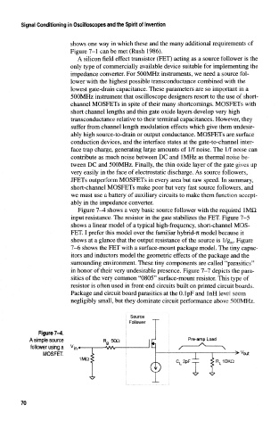
Figure 7-4 shows a very basic source follower with the required 1MQ
input resistance. The resistor in the gate stabilizes the FET. Figure 7-5
shows a linear model of a typical high-frequency, short-channel MOS-
FET. I prefer this model over the familiar hybrid-Tt model because it
shows at a glance that the output resistance of the source is l/g m. Figure
7-6 shows the FET with a surface-mount package model. The tiny capac-
itors and inductors model the geometric effects of the package and the
surrounding environment. These tiny components are called "parasitics"
in honor of their very undesirable presence. Figure 7-7 depicts the para-
sitics of the very common "0805" surface-mount resistor. This type of
resistor is often used in front-end circuits built on printed circuit boards.
Package and circuit board parasitics at the 0.1 pF and InH level seem
negligibly small, but they dominate circuit performance above 500MHz.
Source
I Follower
Figure 7-4.
A simple source R 50Q IK \ P re-amp Load
9 I
follower using a v j n « 1 ^>J\J\j ; ' * —
MOSFET, ; _^ -but
1MO < > I L
\ IVf»4 —
4 ^ C L2pF_._ SR L10KQ
^ : i J
"S 7 \
70