
Page 627 - The Mechatronics Handbook
P. 627
0066_Frame_C20.fm Page 97 Wednesday, January 9, 2002 1:44 PM
theory and mechanics comprise the fundamentals for analysis, modeling, simulation, design, and opti-
mization, while fabrication is based on the micromachining and high-aspect-ratio techniques and pro-
cesses, which are the extension of the CMOS technologies developed to fabricate ICs. For many years,
the developments in microelectromechanical systems (MEMS) have been concentrated on the fabrica-
tion of microstructures adopting, modifying, and redesigning silicon-based processes and technologies
commonly used in integrated microelectronics. The reason for refining of conventional processes and
technologies as well as application of new materials is simple: in general, microstructures are three-
dimensional with high aspect ratios and large structural heights in contrast to two-dimensional planar
microelectronic devices. Silicon structures can be formed from bulk silicon micromachining using wet
or dry processes, or through surface micromachining. Metallic micromolding techniques, based upon
photolithographic processes, are also widely used to fabricate microstructures. Molds are created in
polymer films (usually photoresist) on planar surfaces, and then filled by electrodepositing metal (elec-
trodeposition plays a key role in the fabrication of the microstructures and microdevices, which are the
components of MEMS). High-aspect ratio technologies use optical, e-beam, and x-ray lithography to
create trenches up to 1 mm deep in polymethylmethacrylate resist on the electroplating base (called seed
layer). Electrodeposition of magnetic materials and conductors, electroplating, electroetching, and lift-
off are extremely important processes to fabricate microscale structures and devices. Though it is recog-
nized that the ability to use and refine existing microelectronics fabrication technologies and materials
is very important, and the development of novel processes to fabricate MEMS is a key factor in the rapid
growth of affordable MEMS, other emerging areas arise. In particular, devising, design, modeling,
analysis, and optimization of novel MEMS are extremely important. Therefore, recently, the MEMS
theory and microengineering fundamentals have been expanded to thoroughly study other critical prob-
lems such as the system-level synthesis and integration, synergetic classification and analysis, modeling
and design, as well as optimization. This chapter studies the fabrication, analysis, and design problems
for electromagnetic microstructures and microdevices (microtransducers with ICs). The descriptions of
the fabrication processes are given, modeling and analysis issues are emphasized, and the design is
performed.
Design and Fabrication
In MEMS, the fabrication of thin film magnetic components and microstructures requires deposition of
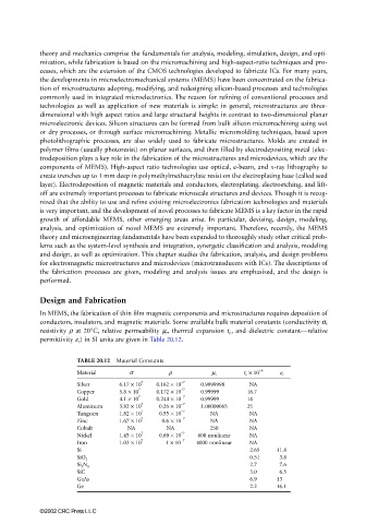
conductors, insulators, and magnetic materials. Some available bulk material constants (conductivity σ,
resistivity ρ at 20°C, relative permeability µ r , thermal expansion t e , and dielectric constant—relative
permittivity r ) in SI units are given in Table 20.12.
TABLE 20.12 Material Constants
Material σ ρ µ r t e × 10 −6 r
7 −7
Silver 6.17 × 10 0.162 × 10 0.9999998 NA
7 −7
Copper 5.8 × 10 0.172 × 10 0.99999 16.7
7 −7
Gold 4.1 × 10 0.244 × 10 0.99999 14
7 −7
Aluminum 3.82 × 10 0.26 × 10 1.00000065 25
7 −7
Tungsten 1.82 × 10 0.55 × 10 NA NA
7 −7
Zinc 1.67 × 10 0.6 × 10 NA NA
Cobalt NA NA 250 NA
7 −7
Nickel 1.45 × 10 0.69 × 10 600 nonlinear NA
7 −7
Iron 1.03 × 10 1 × 10 4000 nonlinear NA
Si 2.65 11.8
0.51 3.8
SiO 2
2.7 7.6
Si 3 N 4
SiC 3.0 6.5
GaAs 6.9 13
Ge 2.2 16.1
©2002 CRC Press LLC