
Page 631 - The Mechatronics Handbook
P. 631
0066_Frame_C20.fm Page 101 Wednesday, January 9, 2002 1:44 PM
oriented sidewalls, the electroplating can be nonuniform. To overcome this problem, the through-holes
can be over-plated and polished to the surface level [5–7]. After the through-hole plating and polishing,
the seed layer is removed, and 10–20 µm coat (e.g., polyimide PI2611) is spun on the backside and cured
at 300°C to cover the protective NiFe layer. Now, the microinductor can be fabricated on the topside of
the wafer. In particular, the microcoils are fabricated on top of the through-hole wafer with the specified
magnetic core geometry (e.g., plate- or horseshoe-shaped) parallel to the surface of the wafer. The
microcoils must be wounded around the magnetic core to form the electromagnetic system. Therefore,
the additional structural layers are needed (for example, the first level is the conductors that are the
bottom segments of each microcoil turn, the second level includes the magnetic core and vertical
conductors which connect the top and bottom of each microcoil turn segment, and the third level consists
of the top conductors that are connected to the electrical vias, and thus form microcoil turns wounded around
the magnetic core). It is obvious that the insulation (dielectric) layers are required to insulate the magnetic
core and microcoils. The fabrication can be performed through the electron beam evaporation of the
Ti-Cu seed layer, and then, 25–35 µm electroplating molds are formed (AZ-4000 photoresist can be
used). The copper microcoils are electroplated on the top of the mold through electroplating. After
electroplating is completed, the photoresist is removed with acetone. Then, the seed layer is removed
(copper is etched in the H 2 SO 4 solution, while the titanium adhesion layer is etched by the HF solution).
A new layer of the AZ-4000 photoresist is spun on the wafer to insulate the bottom conductors from the
magnetic core. The vias’ openings are patterned at the ends of the conductors, and the photoresist is
cured forming the insulation layer. In addition to insulation, the hard curing leads to reflow of the
photoresist serving the planarization purpose needed to pattern additional layers. Another seed layer is
deposited from which electrical vias and magnetic core are patterned and electroplated. This leads to
two lithography sequential steps, and the electrical vias (electroplated Cu) and magnetic core (NiFe thin
film) are electroplated using the same seed layer. After the vias and magnetic core are completed, the
photoresist and seed layers are removed. Then, the hard curing is performed. The top microconductors
are patterned and deposited from another seed layer using the same process as explained above for the
bottom microconductors. The detailed description of the processes described and the fabricated
microtransducers are available in [5–7]. We have outlined the fabrication of microinductors because these
techniques can be adopted and used to fabricate microtransducers. It also must be emphasized that the
analysis and design can be performed using the equations given.
Analysis of Translational Microtransducers
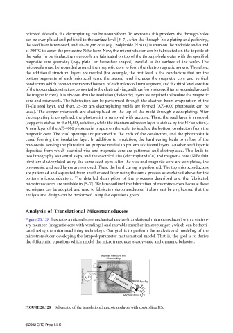
Figure 20.128 illustrates a microelectromechanical device (translational microtransducer) with a station-
ary member (magnetic core with windings) and movable member (microplunger), which can be fabri-
cated using the micromachining technology. Our goal is to perform the analysis and modeling of the
microtransducer developing the lamped-parameter mathematical model. That is, the goal is to derive
the differential equations which model the microtransducer steady-state and dynamic behavior.
FIGURE 20.128 Schematic of the translational microtransducer with controlling ICs.
©2002 CRC Press LLC