
Page 137 - Troubleshooting Analog Circuits
P. 137
I24 IO. The Analog/Digital Boundary
I have made up a list of all these ICs with nonstandard pinouts, and they are in
Appendix A, in the back. . . .
Similarly, some CMOS devices have many-but not all-of their functions in
common with those of their TTL counterparts. For example, the 74C74 has the same
pinout and 95% of the same functions as the TTL 7474. Both follow mostly the same
truth table, except that when you pull both the preset and clear inputs low, the TTL
device’s outputs (Q andq) both go LOW, whereas the CMOS part’s outputs both go
HIGH. If anybody has a complete list of such differences, I’d love to see a copy.
In some cases you can buy a buffered gate (CD4001BN), an unbuffered gate
(CD4001), an unbuffered inverter (MM74HCU04), or a buffered inverter
(MM74HC04). Sometimes, you can buy one part number and get an unbuffered part
from one vendor and a buffered one from another. Of course, the unbuffered parts are
faster with light capacitive loads, but the buffered ones are faster with heavy loads.
So if you have a critical application, be aware that substituting different vendors’
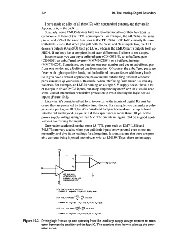
parts can mess up your circuit. Be careful when interfacing from linear ICs into dig-
ital ones. For example, an LM324 running on a single 5-V supply doesn’t have a lot
of margin to drive CMOS inputs, but an op amp running on f5 or f10 V would need
some kind of attenuation or resistive protection to avoid abusing the logic-device
inputs (Figure 10.2).
Likewise, it’s considered bad form to overdrive the inputs of digital ICs just be-
cause they are protected by built-in clamp diodes. For example, you can make a pulse
generator per Figure 10.3, but it’s considered bad practice to drive the inputs hard
into the rail and beyond, as you will if the capacitance is more than 0.01 p,F or the
power supply voltage is higher than 6 V. The circuits in Figure 10.4 do as good a job
without overdriving the inputs.
One reader cautioned me that some LS-TTL parts such as DM74LS86 and
74LS75s are very touchy when you pull their inputs below ground even micro-mo-
mentarily, and give false readings for a long time. It sounds to me that there are prob-
ably currents being injected into tubs, as with an LM339: Thus, these are unhappy
FOR CMOS. RdRZa +VJI-V.l
EXAMPLE +V.-5V, -Vs--5V, R, -Ra-lOk
+ld
FOR TTL, CHOOSE 2-2 mA
EXAMPLE: +Vs -5V. -VI --SV, R, -4.7k. Rs -2.2k
FOR LTTL. CHOOSE N=* +a16 mA
Ra RI
EXAMPLE: +VU -5V. -Vu --5V, R, -4.7k. & -3k
Figure 10.2. Driving logic from an op amp operating from the usual large supply voltages requires an atten-
uator between the amplifier and the logic IC. The equations show how to calculate the atten-
uator ratios.