
Page 93 - Wire Bonding in Microelectronics
P. 93
72 Cha pte r T h ree
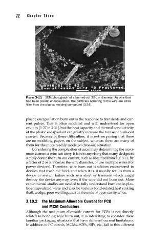
FIGURE 3-11 SEM photograph of a burned-out 25-µm diameter Au wire that
had been plastic encapsulated. The particles adhering to the wire are silica
fi ller from the plastic molding compound [3-34].
plastic encapsulation burn out is the response to transients and cur-
rent pulses. This is often modeled and well understood for open
cavities [3-27 to 3-31], but the heat capacity and thermal conductivity
of the plastic encapsulant can greatly increase the transient burn-out
current. Because of these difficulties, it is not surprising that there
are no modeling papers on the subject, whereas there are many of
them for the more readily modeled (free-air) situation.
Considering the complexities of accurately determining the maxi-
mum current a wire can carry, it is not surprising that many designers
simply derate the burn-out current, such as obtained from Fig. 3-11, by
a factor of 2 or 3, increase the wire diameter, or use multiple wires (for
power devices). Therefore, wire burn out is seldom encountered in
devices that reach the field, and when it is, it usually results from a
device or system failure such as a short or transient which might
destroy the device anyway, even if the wire did not burn out. More
experimental studies are needed to fully understand burn out in plas-
tic-encapsulated wires and also for various bond-related heat sinking
(ball, wedge, poor welding, etc.) at the ends of open cavity wires.
3.10.2 The Maximum Allowable Current for PCB
and MCM Conductors
Although the maximum allowable current for PCBs is not directly
related to bonding wire burn out, it is interesting to consider these
familiar packaging situations that have different current limitations.
In addition to PC boards, MCMs, SOPs, SIPs, etc., fall in this different