
Page 205 - A Comprehensive Guide to Solar Energy Systems
P. 205
Chapter 9 • Crystalline Silicon Solar Cell and Module Technology 207
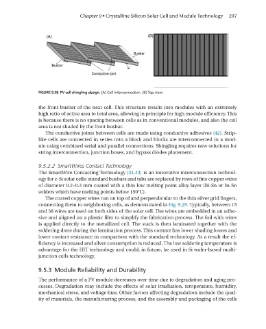
FIGURE 9.28 PV cell shingling design. (A) Cell interconnection. (B) Top view.
the front busbar of the next cell. This structure results into modules with an extremely
high ratio of active area to total area, allowing in principle for high module efficiency. This
is because there is no spacing between cells as in conventional modules, and also the cell
area is not shaded by the front busbar.
The conductive joints between cells are made using conductive adhesives [42]. Strip-
like cells are connected in series into a block and blocks are interconnected in a mod-
ule using combined serial and parallel connections. Shingling requires new solutions for
string interconnection, junction boxes, and bypass diodes placement.
9.5.2.2 SmartWires Contact Technology
The SmartWire Contacting Technology [34,43] is an innovative interconnection technol-
ogy for c-Si solar cells: standard busbars and tabs are replaced by rows of fine copper wires
of diameter 0.2–0.3 mm coated with a thin low melting point alloy layer (Bi-Sn or In-Sn
solders which have melting points below 150°C).
The coated copper wires run on top of and perpendicular to the thin silver grid fingers,
connecting them to neighboring cells, as demonstrated in Fig. 9.29. Typically, between 15
and 38 wires are used on both sides of the solar cell. The wires are embedded in an adhe-
sive and aligned on a plastic film to simplify the fabrication process. The foil with wires
is applied directly to the metallized cell. The stack is then laminated together with the
soldering done during the lamination process. This contact has lower shading losses and
lower contact resistance in comparison with the standard technology. As a result the ef-
ficiency is increased and silver consumption is reduced. The low soldering temperature is
advantage for the hJT technology and could, in future, be used in Si wafer-based multi-
junction cells technology.
9.5.3 Module Reliability and Durability
The performance of a PV module decreases over time due to degradation and aging pro-
cesses. Degradation may include the effects of solar irradiation, temperature, humidity,
mechanical stress, and voltage bias. Other factors affecting degradation include the qual-
ity of materials, the manufacturing process, and the assembly and packaging of the cells