
Page 165 - Advances in Renewable Energies and Power Technologies
P. 165
138 CHAPTER 4 Performance of MPPT Techniques of Photovoltaic Systems
50
Error -50 0
1 1.02 1.04 1.06 1.08 1.1
50
Delta (Error) .0
-50 1 1.02 1.04 1.06 1.08 1.1
Delta Duty Ratio 0.01
.0
-0.01
1 1.02 1.04 1.06 1.08 1.1
0.6
Duty Ratio 0.58
0.56
1 1.02 1.04 1.06 1.08 1.1
32
Optimum Voltage 31
30
29
1 1.02 1.04 1.06 1.08 1.1
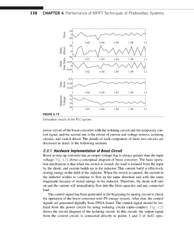
FIGURE 4.19
Simulation results of the FLC system.
power circuit of the boost converter with the isolating circuit and the temporary con-
trol signal, and the second one is the circuit of current and voltage sensors, isolating
circuits, and switch driver. The details of each component of these two circuits are
discussed in detail in the following sections.
2.3.1 Hardware Implementation of Boost Circuit
Boost or step-up converter has an output voltage that is always greater than the input
voltage. Fig. 4.21 shows a conceptual diagram of boost converter. The basic opera-
tion mechanism is that when the switch is closed, the load is isolated from the input
by the diode, and current builds up in the inductor. This current build is effectively
storing energy in the field of the inductor. When the switch is opened, the current in
the inductor wishes to continue to flow in the same direction and with the same
magnitude because of stored energy in the inductor. Therefore, the diode will turn
on and the current will immediately flow into the filter capacitor and any connected
load.
The control signal has been generated in the beginning by analog circuit to check
the operation of the boost converter with PV energy system. After that, the control
signals are generated digitally from FPGA board. The control signal should be iso-
lated from the power circuit by using isolating circuit (opto-coupler). Fig. 4.22
shows the circuit diagram of the isolating circuit. In this circuit, the output signal
from the control circuit is connected directly to points 1 and 2 of 4n32 opto-