
Page 138 - An Introduction to Microelectromechanical Systems Engineering
P. 138
Actuators and Actuated Microsystems 117
microheaters on a silicon chip. High-performance inkjet technology represents an
excellent illustration of how micromachining has become a critical and enabling
element in a more complex system.
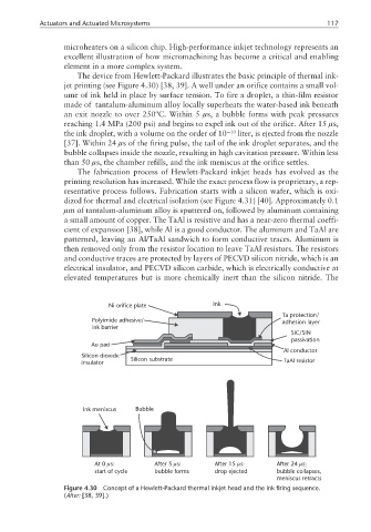
The device from Hewlett-Packard illustrates the basic principle of thermal ink-
jet printing (see Figure 4.30) [38, 39]. A well under an orifice contains a small vol-
ume of ink held in place by surface tension. To fire a droplet, a thin-film resistor
made of tantalum-aluminum alloy locally superheats the water-based ink beneath
an exit nozzle to over 250ºC. Within 5 µs, a bubble forms with peak pressures
reaching 1.4 MPa (200 psi) and begins to expel ink out of the orifice. After 15 µs,
the ink droplet, with a volume on the order of 10 −10 liter, is ejected from the nozzle
[37]. Within 24 µs of the firing pulse, the tail of the ink droplet separates, and the
bubble collapses inside the nozzle, resulting in high cavitation pressure. Within less
than 50 µs, the chamber refills, and the ink meniscus at the orifice settles.
The fabrication process of Hewlett-Packard inkjet heads has evolved as the
printing resolution has increased. While the exact process flow is proprietary, a rep-
resentative process follows. Fabrication starts with a silicon wafer, which is oxi-
dized for thermal and electrical isolation (see Figure 4.31) [40]. Approximately 0.1
µm of tantalum-aluminum alloy is sputtered on, followed by aluminum containing
a small amount of copper. The TaAl is resistive and has a near-zero thermal coeffi-
cient of expansion [38], while Al is a good conductor. The aluminum and TaAl are
patterned, leaving an Al/TaAl sandwich to form conductive traces. Aluminum is
then removed only from the resistor location to leave TaAl resistors. The resistors
and conductive traces are protected by layers of PECVD silicon nitride, which is an
electrical insulator, and PECVD silicon carbide, which is electrically conductive at
elevated temperatures but is more chemically inert than the silicon nitride. The
Ni orifice plate Ink
Ta protection/
Polyimide adhesive/ adhesion layer
ink barrier
SiC/SiN
passivation
Au pad
Al conductor
Silicon dioxide
insulator Silicon substrate TaAl resistor
Ink meniscus Bubble
µ
µ
µ
µ
At 0 s: After 5 s: After 15 s: After 24 s:
start of cycle bubble forms drop ejected bubble collapses,
meniscus retracts
Figure 4.30 Concept of a Hewlett-Packard thermal inkjet head and the ink firing sequence.
(After: [38, 39].)