
Page 139 - An Introduction to Microelectromechanical Systems Engineering
P. 139
118 MEM Structures and Systems in Industrial and Automotive Applications
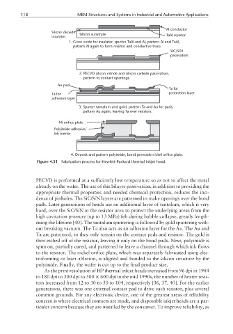
Al conductor
Silicon dioxide
Silicon substrate TaAl resistor
insulator
1. Grow oxide for insulator, sputter TaAl and Al, pattern Al and TaAl,
pattern Al again to form resistor and conductive trace.
SiC/SiN
passivation
2. PECVD silicon nitride and silicon carbide passivation,
pattern to contact openings.
Au pad
Ta for
Ta for protection layer
adhesion layer
3. Sputter tantalum and gold, pattern Ta and Au for pads,
pattern Au again, leaving Ta over resistors.
Ni orifice plate
Polyimide adhesive/
ink barrier
4. Deposit and pattern polyimide, bond premade nickel orifice plate.
Figure 4.31 Fabrication process for Hewlett-Packard thermal inkjet head.
PECVD is performed at a sufficiently low temperature so as not to affect the metal
already on the wafer. The use of this bilayer passivation, in addition to providing the
appropriate thermal properties and needed chemical protection, reduces the inci-
dence of pinholes. The SiC/SiN layers are patterned to make openings over the bond
pads. Later generations of heads use an additional layer of tantalum, which is very
hard, over the SiC/SiN in the resistor area to protect the underlying areas from the
high cavitation pressure (up to 13 MPa) felt during bubble collapse, greatly length-
ening the lifetime [40]. The tantalum sputtering is followed by gold sputtering with-
out breaking vacuum. The Ta also acts as an adhesion layer for the Au. The Au and
Ta are patterned, so they only remain on the contact pads and resistor. The gold is
then etched off of the resistor, leaving it only on the bond pads. Next, polyimide is
spun on, partially cured, and patterned to leave a channel through which ink flows
to the resistor. The nickel orifice plate, which was separately fabricated using elec-
troforming or laser ablation, is aligned and bonded to the silicon structure by the
polyimide. Finally, the wafer is cut up to the final product size.
As the print resolution of HP thermal inkjet heads increased from 96 dpi in 1984
to 180 dpi to 300 dpi to 300 × 600 dpi in the mid 1990s, the number of heater resis-
tors increased from 12 to 30 to 50 to 104, respectively [36, 37, 40]. For the earlier
generations, there was one external contact pad to drive each resistor, plus several
common grounds. For any electronic device, one of the greatest areas of reliability
concern is where electrical contacts are made, and disposable inkjet heads are a par-
ticular concern because they are installed by the consumer. To improve reliability, as