
Page 144 - An Introduction to Microelectromechanical Systems Engineering
P. 144
Actuators and Actuated Microsystems 123
causing it to contract and recover its original undeflected position in the plane of the
third wafer. This action pulls the poppet back from the orifice, hence permitting
fluid flow.
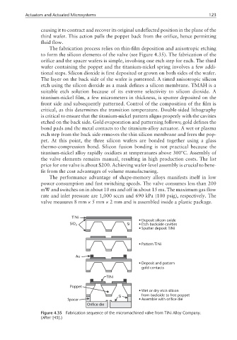
The fabrication process relies on thin-film deposition and anisotropic etching
to form the silicon elements of the valve (see Figure 4.35). The fabrication of the
orifice and the spacer wafers is simple, involving one etch step for each. The third
wafer containing the poppet and the titanium-nickel spring involves a few addi-
tional steps. Silicon dioxide is first deposited or grown on both sides of the wafer.
The layer on the back side of the wafer is patterned. A timed anisotropic silicon
etch using the silicon dioxide as a mask defines a silicon membrane. TMAH is a
suitable etch solution because of its extreme selectivity to silicon dioxide. A
titanium-nickel film, a few micrometers in thickness, is sputter deposited on the
front side and subsequently patterned. Control of the composition of the film is
critical, as this determines the transition temperature. Double-sided lithography
is critical to ensure that the titanium-nickel pattern aligns properly with the cavities
etched on the back side. Gold evaporation and patterning follows; gold defines the
bond pads and the metal contacts to the titanium-alloy actuator. A wet or plasma
etch step from the back side removes the thin silicon membrane and frees the pop-
pet. At this point, the three silicon wafers are bonded together using a glass
thermo-compression bond. Silicon fusion bonding is not practical because the
titanium-nickel alloy rapidly oxidizes at temperatures above 300ºC. Assembly of
the valve elements remains manual, resulting in high production costs. The list
price for one valve is about $200. Achieving wafer-level assembly is crucial to bene-
fit from the cost advantages of volume manufacturing.
The performance advantage of shape-memory alloys manifests itself in low
power consumption and fast switching speeds. The valve consumes less than 200
mW and switches on in about 10 ms and off in about 15 ms. The maximum gas flow
rate and inlet pressure are 1,000 sccm and 690 kPa (100 psig), respectively. The
valve measures 8 mm × 5 mm × 2 mm and is assembled inside a plastic package.
TiNi
• Deposit silicon oxide
SiO 2 Si • Etch backside cavities
• Sputter deposit TiNi
• Pattern TiNi
Au
• Deposit and pattern
gold contacts
TiNi
Poppet
• Wet or dry etch silicon
Si from backside to free poppet
Spacer • Assemble with orifice die
Orifice die
Figure 4.35 Fabrication sequence of the micromachined valve from TiNi Alloy Company.
(After: [45].)