
Page 216 - An Introduction to Microelectromechanical Systems Engineering
P. 216
Passive Electrical Components: Capacitors and Inductors 195
center makes an electrical contact with low resistance and low inductance. The
greatest challenge in this design is fabricating the plate metal with a low residual
stress gradient to avoid curling. For a nominal capacitance of 2 pF, this design has a
Q of 181 at 1 GHz and a self-resonance frequency of 7.5 GHz. The tuning range is
1.45:1 at 5.5V. To demonstrate the deleterious effect of substrate conductivity,
capacitors were fabricated with the same process on fused quartz and on high-
resistivity (>10 kΩ•cm) silicon substrates with 4 µm of silicon dioxide for an insu-
lator. The small parasitic conductance through the silicon reduced Q by a factor of
40 compared to that on quartz. The use of an insulating substrate also reduced the
parasitic capacitance in the traces and bond pads, which was a concern with the
other designs, to about 1% of the nominal capacitance.
All of the surface-micromachined designs described have small etch holes in the
top plate to allow the etchant to remove the sacrificial layer rapidly. The last design
also has a layer of silicon nitride coating the bottom plate to prevent shorting when
the top plate snaps down. It further has standoff bumps protruding under the top
plate to limit motion and reduce the contact area at snap down, reducing the likeli-
hood of sticking.
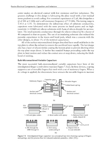
Bulk-Micromachined Variable Capacitors
The most successful bulk-micromachined variable capacitors have been of the
interdigitated-finger (comb-drive) type [see Figure 7.3(a)]. In these devices, a spring
supports a set of movable fingers that mesh with a set of stationary fingers. When a
dc voltage is applied, the electrostatic force attracts the movable fingers to increase
Capacitor gap
Stationary fingers Movable fingers
Folded-beam spring
Anchor and Anchor and
electrical contact electrical contact
Motion
(a)
µ
SOI Thick Si 20- m epoxy 2- m Al
µ
wafer Buried oxide
µ
20- m Si
Glass
1. SOI and glass wafers 2. Bond wafers with epoxy 3. Remove thick Si and
oxide; deposit Al
µ
~0.25- m Al
4. RIE through Al; 5. Etch epoxy, 6. Deposit thin Al
DRIE through Si undercutting Si to coat sidewalls
(b)
Figure 7.3 Interdigitated-finger capacitor: (a) conceptual top view showing a group of fingers
and springs; and (b) process flow for reduced substrate parasitics. (After: [11].)