
Page 218 - An Introduction to Microelectromechanical Systems Engineering
P. 218
Passive Electrical Components: Capacitors and Inductors 197
A further concern for interdigitated-finger capacitors is motion of the movable fin-
gers sideways, perpendicular to the intended direction of travel [along the verti-
cal direction in Figure 7.3(a)]. In this event, the gap on one side is reduced,
and the electrostatic force increases rapidly. This eventually pulls the fingers
together, resulting in an electrical short. The spring constant perpendicular to the
direction of travel must be sufficiently large to prevent any such displacement
under the expected operating conditions. Microphonics is a key concern that
must be resolved before micromachined variable capacitors are fully deployed in
commercial systems.
Micromachined Inductors
Billions of low-cost discrete inductors are sold annually for applications including
RF filters, VCOs, and chokes. Most of these have inductances in the range of a few
to tens of nanohenries. When used in conjunction with an integrated circuit, discrete
circuit components suffer from parasitic capacitance in traces and bond pads on the
chip, in the bond wires connecting the chip to the circuit board, and in the inductor
packaging. This limits the self-resonance frequency and therefore the maximum
operating frequency. The inductors also consume precious board space in portable
electronics; for example, in a Nokia 6161 cellular telephone, there are 24 discrete
inductors (in addition to even more capacitors and resistors) along with only 15
integrated circuits [12]. To alleviate the self-resonance shortcoming and to reduce
the part count and space used on a printed circuit board, low-cost, high-
performance on-chip inductors are desirable.
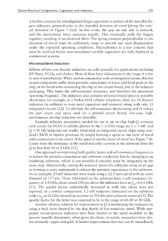
Example inductor parameters needed for use in an on-chip high-Q resonant
tank circuit for VCOs in cellular phones in the 1–2 GHz range are L =5nH and
Q >30 [4]. Inductors are readily fabricated on integrated-circuit chips using stan-
dard CMOS or bipolar processes by simply forming a spiral in one layer of metal
and a connection to the center of the spiral in another layer of metal (see Figure 7.4).
Losses from the resistance of the metal and eddy currents in the substrate limit the
Q to less than 10 at 2 GHz [11].
One approach to improving both quality factor and self-resonance frequency is
to reduce the parasitic capacitance and substrate conductive loss by changing to an
insulating substrate, which is not possible if circuitry must be integrated on the
same chip. Alternatively, raising the inductor above the substrate using an air gap
or forming a cavity underneath it reduces the parasitic capacitance to the substrate.
As an example, 24-nH inductors were made using a 12.5-turn spiral with an outer
diameter of 137 µm. Those fabricated on the substrate have a self-resonance fre-
quency of 1.8 GHz; those raised 250 µm above the substrate have an f of 6.6 GHz
SR
[11]. The quality factor undoubtedly increased as well, but values were not
reported. In a similar comparison, 1.2-nH inductors fabricated on the substrate
with a f of 22 GHz showed an increase to 70 GHz after substrate removal [3]. The
SR
quality factor for the latter was expected to be in the range of 60–80 at 40 GHz.
Another obvious solution for improvement in Q is minimizing the resistance by
using a thick layer (limited by the skin depth) of low-resistivity metal. While inte-
grated circuit–process inductors have been limited to the metal available in the
process (usually aluminum), when given the choice of metals, researchers have cho-
sen primarily copper and gold. A further improvement that may not be immediately