
Page 219 - An Introduction to Microelectromechanical Systems Engineering
P. 219
198 MEM Structures and Systems in RF Applications
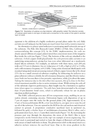
Lower metal
Parasitic capacitance
coil inductor
between turns
Insulated
substrate
Parasitic capacitance
to substrate
Upper metal connector
(on dielectric)
Parasitic conductance in substrate
Figure 7.4 Illustration of a planar on-chip inductor, with parasitics noted. The inductor consists
of a planar spiral made in one layer of metal and a connection to the center of the spiral in another
layer of metal.
apparent is the addition of a highly conductive ground plane under the coil. Eddy
currents are still induced, but the losses are much lower than with a resistive material.
An alternative to planar spiral inductors is positioning small solenoids on top of
the substrate. The Palo Alto Research Center (PARC) of Palo Alto, California, is
commercializing this concept [13]. In the PARC implementation, the coils are
closely spaced ribbons of copper-plated metal that concentrate most of the magnetic
flux inside the coils [see Figure 7.5(a)]. The bottoms of the coils are attached to the
substrate. A thick copper shield placed under the coils prevents eddy currents in an
underlying semiconductor, giving low loss even when fabricated on a moderately
doped silicon substrate. For example, an inductor with three turns, each 200 µm
wide and 535 µm in diameter, has an inductance of 4 nH, a high Q of 65 at 1 GHz,
and a self-resonance frequency of 4.2 GHz. Using a thin aluminum shield made with
standard integrated circuit processing instead of thick copper lowers the Q by about
25% due to a small amount of substrate coupling. By fabricating the inductor on a
glass substrate without a shield, the self-resonance frequency and the effective induc-
tance both rise because there is less parasitic capacitance, while Q is about the same.
Taking the resistance due to the skin effect into account, this Q is close to the theo-
retical maximum possible to due to series resistance alone. While raising the coils off
of the substrate improves performance, their height may be a limitation in applica-
tions where space is a constraint. The coils have been demonstrated to be stronger
than 25-µm-diameter bond wires, which is sufficiently robust for use in plastic
injection-molded packages.
The PARC solenoid process uses all low-temperature steps, enabling its use on
wafers already containing circuitry. Fabrication begins with deposition of up to
7 µm of copper onto the wafer for the ground plane [14]. Approximately 12 to
15 µm of benzocyclobutene (BCB), a low-loss dielectric, are spun on to raise the coil
up off of the substrate. Vias are opened in the BCB for the coil anchors and electrical
contact to ground. A proprietary conductive sacrificial layer is sputtered on,
followed by gold, a thicker layer of molybdenum-chromium (MoCr) alloy, and a
gold passivation layer, for a 1.5-µm-thick metal stack (Figure 7.6). By increasing the
pressure part way through the deposition, the stress of the MoCr film is more
compressive on the bottom than on the top—an example of stress engineering. The
metal stack is patterned and etched to form the shapes of flattened coil half-turns,
with arrays of small etch holes in them. The photoresist is left on the metal stack as a
selective etchant removes the sacrificial layer. Due to the stress gradient in the