
Page 220 - An Introduction to Microelectromechanical Systems Engineering
P. 220
Passive Electrical Components: Capacitors and Inductors 199
µ
µ
300 m 100 m
(a) (b)
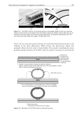
Figure 7.5 The PARC inductor: (a) scanning-electron micrograph (SEM) of a five-turn solenoid
inductor (the locations of the sides of the turns before release are visible); and (b) SEM close up of
the tops of the turns where the metal from each side meets, showing the interlocked ends. The
etch holes have been filled with copper. (© 2003 IEEE [13].)
MoCr, the free ends curl upward, but do not reach their final destination due to the
stiffness of the thick photoresist. When heated, the photoresist softens and
gradually allows the free ends to bend further. By precisely controlling the stress
gradient and the thickness of the MoCr film, the radius of curvature is such that the
Photoresist
Au/MoCr/Au
Sacrificial layer
BCB dielectric
Cu ground plane
Substrate
1. Deposit Cu ground plane. Deposit and pattern dielectric.
Sputter sacrificial metal and Au/MoCr/Au stack with stress gradient in MoCr.
Pattern metal with photoresist and etch.
MoCr film curls up
2. Etch sacrificial layer to release MoCr film, which curls slightly.
Heat to relax photoresist. Au/MoCr/Au stack curls completely.
3. Strip photoresist.
Electroplate Au/MoCr/Au with copper.
Figure 7.6 Illustration of the PARC inductor fabrication process.